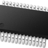
PIC24FJ64GB002-I/SS Microchip Technology, PIC24FJ64GB002-I/SS Datasheet - Page 291

PIC24FJ64GB002-I/SS
Manufacturer Part Number
PIC24FJ64GB002-I/SS
Description
16-bit, 16 MIPS, 64KB Flash, 8KB RAM, Nanowatt XLP, USB OTG 28 SSOP .209in TUBE
Manufacturer
Microchip Technology
Specifications of PIC24FJ64GB002-I/SS
Processor Series
PIC24
Core
PIC24F
Data Bus Width
16 bit
Program Memory Type
Flash
Program Memory Size
64 KB
Data Ram Size
8192 B
Interface Type
I2C, SPI, UART
Maximum Clock Frequency
32 MHz
Number Of Programmable I/os
21
Number Of Timers
5
Operating Supply Voltage
2 V to 3.6 V
Maximum Operating Temperature
+ 85 C
Mounting Style
SMD/SMT
Package / Case
SSOP-28
Development Tools By Supplier
MPLAB Integrated Development Environment
Minimum Operating Temperature
- 40 C
Operating Temperature Range
- 40 C to + 85 C
Supply Current (max)
300 mA
Lead Free Status / Rohs Status
Lead free / RoHS Compliant
Available stocks
Company
Part Number
Manufacturer
Quantity
Price
Part Number:
PIC24FJ64GB002-I/SS
Manufacturer:
MICROCHIP/微芯
Quantity:
20 000
- Current page: 291 of 352
- Download datasheet (3Mb)
26.6
PIC24FJ64GB004 family devices implement a JTAG
interface, which supports boundary scan device
testing.
26.7
PIC24FJ64GB004 family microcontrollers can be seri-
ally programmed while in the end application circuit.
This is simply done with two lines for clock (PGECx)
and data (PGEDx), and three other lines for power,
ground and the programming voltage. This allows cus-
tomers to manufacture boards with unprogrammed
devices and then program the microcontroller just
before shipping the product. This also allows the most
recent firmware or a custom firmware to be
programmed.
2010 Microchip Technology Inc.
JTAG Interface
In-Circuit Serial Programming
PIC24FJ64GB004 FAMILY
26.8
When MPLAB
in-circuit debugging functionality is enabled. This func-
tion allows simple debugging functions when used with
MPLAB IDE. Debugging functionality is controlled
through the PGECx (Emulation/Debug Clock) and
PGEDx (Emulation/Debug Data) pins.
To use the in-circuit debugger function of the device,
the design must implement ICSP connections to
MCLR, V
ignated by the ICS Configuration bits. In addition, when
the feature is enabled, some of the resources are not
available for general use. These resources include the
first 80 bytes of data RAM and two I/O pins.
In-Circuit Debugger
DD
, V
®
SS
ICD 2 is selected as a debugger, the
and the PGECx/PGEDx pin pair des-
DS39940D-page 291
Related parts for PIC24FJ64GB002-I/SS
Image
Part Number
Description
Manufacturer
Datasheet
Request
R

Part Number:
Description:
Manufacturer:
Microchip Technology Inc.
Datasheet:

Part Number:
Description:
Manufacturer:
Microchip Technology Inc.
Datasheet:

Part Number:
Description:
Manufacturer:
Microchip Technology Inc.
Datasheet:

Part Number:
Description:
Manufacturer:
Microchip Technology Inc.
Datasheet:

Part Number:
Description:
Manufacturer:
Microchip Technology Inc.
Datasheet:

Part Number:
Description:
Manufacturer:
Microchip Technology Inc.
Datasheet:

Part Number:
Description:
Manufacturer:
Microchip Technology Inc.
Datasheet:

Part Number:
Description:
Manufacturer:
Microchip Technology Inc.
Datasheet:


