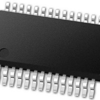
PIC24FJ64GB002-I/SS Microchip Technology, PIC24FJ64GB002-I/SS Datasheet - Page 279

PIC24FJ64GB002-I/SS
Manufacturer Part Number
PIC24FJ64GB002-I/SS
Description
16-bit, 16 MIPS, 64KB Flash, 8KB RAM, Nanowatt XLP, USB OTG 28 SSOP .209in TUBE
Manufacturer
Microchip Technology
Specifications of PIC24FJ64GB002-I/SS
Processor Series
PIC24
Core
PIC24F
Data Bus Width
16 bit
Program Memory Type
Flash
Program Memory Size
64 KB
Data Ram Size
8192 B
Interface Type
I2C, SPI, UART
Maximum Clock Frequency
32 MHz
Number Of Programmable I/os
21
Number Of Timers
5
Operating Supply Voltage
2 V to 3.6 V
Maximum Operating Temperature
+ 85 C
Mounting Style
SMD/SMT
Package / Case
SSOP-28
Development Tools By Supplier
MPLAB Integrated Development Environment
Minimum Operating Temperature
- 40 C
Operating Temperature Range
- 40 C to + 85 C
Supply Current (max)
300 mA
Lead Free Status / Rohs Status
Lead free / RoHS Compliant
Available stocks
Company
Part Number
Manufacturer
Quantity
Price
Part Number:
PIC24FJ64GB002-I/SS
Manufacturer:
MICROCHIP/微芯
Quantity:
20 000
- Current page: 279 of 352
- Download datasheet (3Mb)
26.0
PIC24FJ64GB004 family devices include several
features intended to maximize application flexibility and
reliability, and minimize cost through elimination of
external components. These are:
• Flexible Configuration
• Watchdog Timer (WDT)
• Code Protection
• JTAG Boundary Scan Interface
• In-Circuit Serial Programming
• In-Circuit Emulation
26.1
The Configuration bits can be programmed (read as ‘0’),
or left unprogrammed (read as ‘1’), to select various
device configurations. These bits are mapped starting at
program memory location F80000h. A detailed explana-
tion of the various bit functions is provided in
Register 26-1 through Register 26-6.
Note that address F80000h is beyond the user program
memory space. In fact, it belongs to the configuration
memory space (800000h-FFFFFFh) which can only be
accessed using table reads and table writes.
TABLE 26-1:
2010 Microchip Technology Inc.
PIC24FJ32GB00X
PIC24FJ64GB00X
Note:
Device
SPECIAL FEATURES
Configuration Bits
This data sheet summarizes the features
of this group of PIC24F devices. It is not
intended to be a comprehensive reference
source. For more information, refer to the
following sections of the “PIC24F Family
Reference Manual”:
• Section 9. “Watchdog Timer (WDT)”
• Section 32. “High-Level Device
• Section 33. “Programming and
(DS39697)
Integration” (DS39719)
Diagnostics” (DS39716)
FLASH CONFIGURATION WORD LOCATIONS FOR PIC24FJ64GB004 FAMILY
DEVICES
ABFEh
57FEh
1
PIC24FJ64GB004 FAMILY
Configuration Word Addresses
ABFCh
57FCh
2
26.1.1
In PIC24FJ64GB004 family devices, the configuration
bytes are implemented as volatile memory. This means
that configuration data must be programmed each time
the device is powered up. Configuration data is stored
in the three words at the top of the on-chip program
memory space, known as the Flash Configuration
Words. Their specific locations are shown in
Table 26-1. These are packed representations of the
actual device Configuration bits, whose actual
locations are distributed among several locations in
configuration space. The configuration data is automat-
ically loaded from the Flash Configuration Words to the
proper Configuration registers during device Resets.
When creating applications for these devices, users
should always specifically allocate the location of the
Flash Configuration Word for configuration data. This is
to make certain that program code is not stored in this
address when the code is compiled.
The upper byte of all Flash Configuration Words in
program memory should always be ‘1111 1111’. This
makes them appear to be NOP instructions in the
remote event that their locations are ever executed by
accident. Since Configuration bits are not implemented
in the corresponding locations, writing ‘1’s to these
locations has no effect on device operation.
Note:
Note:
operations on the last page of program
CONSIDERATIONS FOR
CONFIGURING PIC24FJ64GB004
FAMILY DEVICES
Configuration data is reloaded on all types
of device Resets.
Performing a page erase operation on the
last page of program memory clears the
Flash Configuration Words, enabling code
protection as a result. Therefore, users
should avoid performing page erase
memory.
ABFAh
57FAh
3
DS39940D-page 279
ABF8h
57F8h
4
Related parts for PIC24FJ64GB002-I/SS
Image
Part Number
Description
Manufacturer
Datasheet
Request
R

Part Number:
Description:
Manufacturer:
Microchip Technology Inc.
Datasheet:

Part Number:
Description:
Manufacturer:
Microchip Technology Inc.
Datasheet:

Part Number:
Description:
Manufacturer:
Microchip Technology Inc.
Datasheet:

Part Number:
Description:
Manufacturer:
Microchip Technology Inc.
Datasheet:

Part Number:
Description:
Manufacturer:
Microchip Technology Inc.
Datasheet:

Part Number:
Description:
Manufacturer:
Microchip Technology Inc.
Datasheet:

Part Number:
Description:
Manufacturer:
Microchip Technology Inc.
Datasheet:

Part Number:
Description:
Manufacturer:
Microchip Technology Inc.
Datasheet:


