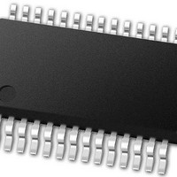
PIC24FJ64GB002-I/SS Microchip Technology, PIC24FJ64GB002-I/SS Datasheet - Page 14

PIC24FJ64GB002-I/SS
Manufacturer Part Number
PIC24FJ64GB002-I/SS
Description
16-bit, 16 MIPS, 64KB Flash, 8KB RAM, Nanowatt XLP, USB OTG 28 SSOP .209in TUBE
Manufacturer
Microchip Technology
Specifications of PIC24FJ64GB002-I/SS
Processor Series
PIC24
Core
PIC24F
Data Bus Width
16 bit
Program Memory Type
Flash
Program Memory Size
64 KB
Data Ram Size
8192 B
Interface Type
I2C, SPI, UART
Maximum Clock Frequency
32 MHz
Number Of Programmable I/os
21
Number Of Timers
5
Operating Supply Voltage
2 V to 3.6 V
Maximum Operating Temperature
+ 85 C
Mounting Style
SMD/SMT
Package / Case
SSOP-28
Development Tools By Supplier
MPLAB Integrated Development Environment
Minimum Operating Temperature
- 40 C
Operating Temperature Range
- 40 C to + 85 C
Supply Current (max)
300 mA
Lead Free Status / Rohs Status
Lead free / RoHS Compliant
Available stocks
Company
Part Number
Manufacturer
Quantity
Price
Part Number:
PIC24FJ64GB002-I/SS
Manufacturer:
MICROCHIP/微芯
Quantity:
20 000
- Current page: 14 of 352
- Download datasheet (3Mb)
PIC24FJ64GB004 FAMILY
TABLE 1-2:
DS39940D-page 14
CN0
CN1
CN2
CN3
CN4
CN5
CN6
CN7
CN8
CN9
CN10
CN11
CN12
CN13
CN15
CN16
CN17
CN18
CN19
CN20
CN21
CN22
CN23
CN25
CN26
CN27
CN28
CN29
CN30
CTED1
CTED2
CV
D+
D-
DMH
DMLN
DPH
DPLN
DISVREG
Legend:
Function
REF
TTL = TTL input buffer
ANA = Analog level input/output
SOIC/SSOP
SPDIP/
28-Pin
12
26
25
24
22
21
18
17
16
14
10
25
21
22
19
11
—
—
—
—
—
—
—
—
—
—
PIC24FJ64GB004 FAMILY PINOUT DESCRIPTIONS (CONTINUED)
2
3
4
5
6
7
9
2
3
5
7
4
6
Pin Number
28-Pin
QFN
27
28
23
22
21
19
18
15
14
13
11
27
28
22
18
19
16
—
—
—
—
—
—
—
—
—
—
9
8
1
2
3
4
7
6
2
4
1
3
QFN/TQFP
44-Pin
34
33
19
20
21
22
23
24
25
26
27
15
14
44
43
37
38
41
36
31
30
19
20
14
22
24
21
23
11
9
8
3
2
5
4
1
8
9
6
I/O
I/O
I/O
O
O
O
O
O
I
I
I
I
I
I
I
I
I
I
I
I
I
I
I
I
I
I
I
I
I
I
I
I
I
I
I
I
I
I
I
I
Buffer
Input
ANA
ANA
ST
ST
ST
ST
ST
ST
ST
ST
ST
ST
ST
ST
ST
ST
ST
ST
ST
ST
ST
ST
ST
ST
ST
ST
ST
ST
ST
ST
ST
ST
—
—
—
—
—
—
—
ST = Schmitt Trigger input buffer
I
2
C™ = I
Interrupt-on-Change Inputs.
CTMU External Edge Input 1.
CTMU External Edge Input 2.
Comparator Voltage Reference Output.
USB Differential Plus Line (internal transceiver).
USB Differential Minus Line (internal transceiver).
D- External Pull-up Control Output.
D- External Pull-down Control Output.
D+ External Pull-up Control Output.
D+ External Pull-down Control Output.
Voltage Regulator Disable.
2
C/SMBus input buffer
Description
2010 Microchip Technology Inc.
Related parts for PIC24FJ64GB002-I/SS
Image
Part Number
Description
Manufacturer
Datasheet
Request
R

Part Number:
Description:
Manufacturer:
Microchip Technology Inc.
Datasheet:

Part Number:
Description:
Manufacturer:
Microchip Technology Inc.
Datasheet:

Part Number:
Description:
Manufacturer:
Microchip Technology Inc.
Datasheet:

Part Number:
Description:
Manufacturer:
Microchip Technology Inc.
Datasheet:

Part Number:
Description:
Manufacturer:
Microchip Technology Inc.
Datasheet:

Part Number:
Description:
Manufacturer:
Microchip Technology Inc.
Datasheet:

Part Number:
Description:
Manufacturer:
Microchip Technology Inc.
Datasheet:

Part Number:
Description:
Manufacturer:
Microchip Technology Inc.
Datasheet:


