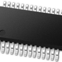
PIC24FJ64GB002-I/SS Microchip Technology, PIC24FJ64GB002-I/SS Datasheet - Page 274

PIC24FJ64GB002-I/SS
Manufacturer Part Number
PIC24FJ64GB002-I/SS
Description
16-bit, 16 MIPS, 64KB Flash, 8KB RAM, Nanowatt XLP, USB OTG 28 SSOP .209in TUBE
Manufacturer
Microchip Technology
Specifications of PIC24FJ64GB002-I/SS
Processor Series
PIC24
Core
PIC24F
Data Bus Width
16 bit
Program Memory Type
Flash
Program Memory Size
64 KB
Data Ram Size
8192 B
Interface Type
I2C, SPI, UART
Maximum Clock Frequency
32 MHz
Number Of Programmable I/os
21
Number Of Timers
5
Operating Supply Voltage
2 V to 3.6 V
Maximum Operating Temperature
+ 85 C
Mounting Style
SMD/SMT
Package / Case
SSOP-28
Development Tools By Supplier
MPLAB Integrated Development Environment
Minimum Operating Temperature
- 40 C
Operating Temperature Range
- 40 C to + 85 C
Supply Current (max)
300 mA
Lead Free Status / Rohs Status
Lead free / RoHS Compliant
Available stocks
Company
Part Number
Manufacturer
Quantity
Price
Part Number:
PIC24FJ64GB002-I/SS
Manufacturer:
MICROCHIP/微芯
Quantity:
20 000
- Current page: 274 of 352
- Download datasheet (3Mb)
PIC24FJ64GB004 FAMILY
REGISTER 24-1:
DS39940D-page 274
bit 15
bit 7
Legend:
R = Readable bit
-n = Value at POR
bit 15-11
bit 10
bit 9-8
bit 7
bit 6
bit 5
bit 4
bit 3-0
CVREN
R/W-0
U-0
—
Unimplemented: Read as ‘0’
CVREFP: C
1 = Use V
0 = Use comparator voltage reference module’s generated output as C
CVREFM<1:0>: CV
11 = Use V
10 = Use V
01 = Use V
00 = Use V
CVREN: Comparator Voltage Reference Enable bit
1 = CV
0 = CV
CVROE: Comparator V
1 = CV
0 = CV
CVRR: Comparator V
1 = CV
0 = CV
CVRSS: Comparator V
1 = Comparator reference source, CV
0 = Comparator reference source, CV
CVR<3:0>: Comparator V
When CVRR = 1:
CV
When CVRR = 0:
CV
CVROE
REF
REF
R/W-0
comparators
U-0
—
CVRCON: COMPARATOR VOLTAGE REFERENCE CONTROL REGISTER
= (CVR<3:0>/24) (CV
= 1/4 (CV
REF
REF
REF
REF
RSRC
RSRC
REF
circuit is powered on
circuit is powered down
voltage level is output on CV
voltage level is disconnected from CV
VREF
REF
BG
BG
BG
range should be 0 to 0.625 CV
range should be 0.25 to 0.719 CV
+ input pin as C
W = Writable bit
‘1’ = Bit is set
/6 as CV
/2 as CV
as CV
+ input pin as CV
+ Reference Output Select bit
R/W-0
CVRR
RSRC
U-0
REF
—
REF
REF
REF
REF
- Reference Output Select bits
) + (CVR<3:0>/32) (CV
REF
REF
- reference output to comparators
Range Selection bit
REF
- reference output to comparators
- reference output to comparators
Source Selection bit
Output Enable bit
VREF
Value Selection (0 CVR<3:0> 15) bits
RSRC
CVRSS
R/W-0
REF
U-0
—
+ reference output to comparators
)
- reference output to comparators
RSRC
RSRC
REF
RSRC
U = Unimplemented bit, read as ‘0’
‘0’ = Bit is cleared
= V
= AV
pin
RSRC
REF
R/W-0
CVR3
RSRC
DD
U-0
REF
—
with CV
+ – V
– AV
with CV
)
pin
REF
SS
RSRC
-
RSRC
CVREFP
R/W-0
R/W-0
CVR2
/24 step size
/32 step size
2010 Microchip Technology Inc.
x = Bit is unknown
VREF
CVREFM1
R/W-0
R/W-0
CVR1
+ reference output to
CVREFM0
R/W-0
R/W-0
CVR0
bit 8
bit 0
Related parts for PIC24FJ64GB002-I/SS
Image
Part Number
Description
Manufacturer
Datasheet
Request
R

Part Number:
Description:
Manufacturer:
Microchip Technology Inc.
Datasheet:

Part Number:
Description:
Manufacturer:
Microchip Technology Inc.
Datasheet:

Part Number:
Description:
Manufacturer:
Microchip Technology Inc.
Datasheet:

Part Number:
Description:
Manufacturer:
Microchip Technology Inc.
Datasheet:

Part Number:
Description:
Manufacturer:
Microchip Technology Inc.
Datasheet:

Part Number:
Description:
Manufacturer:
Microchip Technology Inc.
Datasheet:

Part Number:
Description:
Manufacturer:
Microchip Technology Inc.
Datasheet:

Part Number:
Description:
Manufacturer:
Microchip Technology Inc.
Datasheet:


