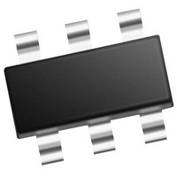
PIC10F322T-I/OT Microchip Technology, PIC10F322T-I/OT Datasheet - Page 150

PIC10F322T-I/OT
Manufacturer Part Number
PIC10F322T-I/OT
Description
896 B Flash, 64 B RAM, 4 I/O, 8bit ADC, PWM, CLC, DDS, CWG, TEMP Indicator, 2.3V
Manufacturer
Microchip Technology
Datasheet
1.PIC10F320-IOT.pdf
(210 pages)
Specifications of PIC10F322T-I/OT
Core
RISC
Processor Series
PIC10F
Data Bus Width
8 bit
Maximum Clock Frequency
31 KHz
Program Memory Size
512 B
Data Ram Size
64 B
Number Of Programmable I/os
4
Number Of Timers
2
Operating Temperature Range
- 40 C to + 85 C
Package / Case
SOT-23-6
Mounting Style
SMD/SMT
Maximum Operating Temperature
+ 85 C
Program Memory Type
Flash
Lead Free Status / Rohs Status
Details
Available stocks
Company
Part Number
Manufacturer
Quantity
Price
Company:
Part Number:
PIC10F322T-I/OT
Manufacturer:
VISHAY
Quantity:
11 490
Part Number:
PIC10F322T-I/OT
Manufacturer:
MICROCHIP/微芯
Quantity:
20 000
- Current page: 150 of 210
- Download datasheet (2Mb)
PIC10(L)F320/322
REGISTER 21-2:
DS41585A-page 150
bit 7
Legend:
R = Readable bit
u = Bit is unchanged
‘1’ = Bit is set
bit 7-6
bit 5-4
bit 3-2
bit 1-0
R/W-x/u
GxASDLB<1:0>
GxASDLB<1:0>: CWGx Shutdown State for CWGxB
When an auto shutdown event is present (GxASE = 1):
11 = CWGxB pin is driven to ‘1’, regardless of the setting of the GxPOLB bit.
10 = CWGxB pin is driven to ‘0’, regardless of the setting of the GxPOLB bit.
01 = CWGxB pin is tri-stated
00 = CWGxB pin is driven to its inactive state after the selected dead-band interval. GxPOLB still will
GxASDLA<1:0>: CWGx Shutdown State for CWGxA
When an auto shutdown event is present (GxASE = 1):
00 = CWGxA pin is driven to its inactive state after the selected dead-band interval. GxPOLA still will
01 = CWGxA pin is tri-stated
10 = CWGxA pin is driven to ‘0’, regardless of the setting of the GxPOLA bit.
11 = CWGxA pin is driven to ‘1’, regardless of the setting of the GxPOLA bit.
Unimplemented: Read as ‘0’
GxIS<1:0>: CWGx Dead-band Source Select bits
11 = LC1OUT
10 = N1OUT
01 = PWM2OUT
00 = PWM1OUT
R/W-x/u
control the polarity of the output.
control the polarity of the output.
CWGxCON1: CWG CONTROL REGISTER 1
W = Writable bit
x = Bit is unknown
‘0’ = Bit is cleared
R/W-x/u
GxASDLA<1:0>
R/W-x/u
Preliminary
U = Unimplemented bit, read as ‘0’
-n/n = Value at POR and BOR/Value at all other Resets
q = Value depends on condition
U-0
—
U-0
—
2011 Microchip Technology Inc.
R/W-0/0
GxIS<1:0>
R/W-0/0
bit 0
Related parts for PIC10F322T-I/OT
Image
Part Number
Description
Manufacturer
Datasheet
Request
R

Part Number:
Description:
896 B Flash, 64 B RAM, 4 I/O, 8bit ADC, PWM, CLC, DDS, CWG, TEMP Indicator, 2.3V
Manufacturer:
Microchip Technology

Part Number:
Description:
896 B Flash, 64 B RAM, 4 I/O, 8bit ADC, PWM, CLC, DDS, CWG, TEMP Indicator, 2.3V
Manufacturer:
Microchip Technology

Part Number:
Description:
896 B Flash, 64 B RAM, 4 I/O, 8bit ADC, PWM, CLC, DDS, CWG, TEMP Indicator, 2.3V
Manufacturer:
Microchip Technology

Part Number:
Description:
896 B Flash, 64 B RAM, 4 I/O, 8bit ADC, PWM, CLC, DDS, CWG, TEMP Indicator, 2.3V
Manufacturer:
Microchip Technology

Part Number:
Description:
896 B Flash, 64 B RAM, 4 I/O, 8bit ADC, PWM, CLC, DDS, CWG, TEMP Indicator, 2.3V
Manufacturer:
Microchip Technology

Part Number:
Description:
896 B Flash, 64 B RAM, 4 I/O, 8bit ADC, PWM, CLC, DDS, CWG, TEMP Indicator, 2.3V
Manufacturer:
Microchip Technology

Part Number:
Description:
384B Flash, 16B RAM, 4 I/O, 8bit ADC 6 SOT-23 BAG
Manufacturer:
Microchip Technology
Datasheet:

Part Number:
Description:
768B Flash, 23B RAM, 4 I/O, 8bit ADC 6 SOT-23 BAG
Manufacturer:
Microchip Technology
Datasheet:

Part Number:
Description:
384B Flash, 16B RAM, 4 I/O, 8bit ADC 6 SOT-23 BAG
Manufacturer:
Microchip Technology
Datasheet:

Part Number:
Description:
768B Flash, 23B RAM, 4 I/O, 8bit ADC 6 SOT-23 BAG
Manufacturer:
Microchip Technology
Datasheet:

Part Number:
Description:
PIC10F PROGRAMMER ADAPTER (SOT-23), PICKIT
Manufacturer:
Microchip Technology Inc.

Part Number:
Description:
Manufacturer:
Microchip Technology Inc.
Datasheet:

Part Number:
Description:
Manufacturer:
Microchip Technology Inc.
Datasheet:


