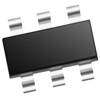
PIC10F322T-I/OT Microchip Technology, PIC10F322T-I/OT Datasheet - Page 60

PIC10F322T-I/OT
Manufacturer Part Number
PIC10F322T-I/OT
Description
896 B Flash, 64 B RAM, 4 I/O, 8bit ADC, PWM, CLC, DDS, CWG, TEMP Indicator, 2.3V
Manufacturer
Microchip Technology
Datasheet
1.PIC10F320-IOT.pdf
(210 pages)
Specifications of PIC10F322T-I/OT
Core
RISC
Processor Series
PIC10F
Data Bus Width
8 bit
Maximum Clock Frequency
31 KHz
Program Memory Size
512 B
Data Ram Size
64 B
Number Of Programmable I/os
4
Number Of Timers
2
Operating Temperature Range
- 40 C to + 85 C
Package / Case
SOT-23-6
Mounting Style
SMD/SMT
Maximum Operating Temperature
+ 85 C
Program Memory Type
Flash
Lead Free Status / Rohs Status
Details
Available stocks
Company
Part Number
Manufacturer
Quantity
Price
Company:
Part Number:
PIC10F322T-I/OT
Manufacturer:
VISHAY
Quantity:
11 490
Part Number:
PIC10F322T-I/OT
Manufacturer:
MICROCHIP/微芯
Quantity:
20 000
- Current page: 60 of 210
- Download datasheet (2Mb)
PIC10(L)F320/322
9.2.2
The unlock sequence is a mechanism that protects the
Flash program memory from unintended self-write pro-
gramming or erasing. The sequence must be executed
and completed without interruption to successfully
complete any of the following operations:
• Row Erase
• Load program memory write latches
• Write of program memory write latches to pro-
• Write of program memory write latches to User
The unlock sequence consists of the following steps:
1. Write 55h to PMCON2
2. Write AAh to PMCON2
3. Set the WR bit in PMCON1
4. NOP instruction
5. NOP instruction
Once the WR bit is set, the processor will always force
two NOP instructions. When an Erase Row or Program
Row operation is being performed, the processor will stall
internal operations (typical 2 ms), until the operation is
complete and then resume with the next instruction.
When the operation is loading the program memory write
latches, the processor will always force the two NOP
instructions and continue uninterrupted with the next
instruction.
Since the unlock sequence must not be interrupted,
global interrupts should be disabled prior to the unlock
sequence and re-enabled after the unlock sequence is
completed.
DS41585A-page 60
gram memory
IDs
FLASH MEMORY UNLOCK
SEQUENCE
Preliminary
FIGURE 9-3:
Instruction Fetched ignored
Instruction Fetched ignored
Write or Erase operation
NOP execution forced
NOP execution forced
Unlock Sequence
Unlock Sequence
Write 0AAh to
Write 055h to
FLASH PROGRAM
MEMORY UNLOCK
SEQUENCE FLOWCHART
PMCON2
PMCON2
(WR = 1)
2011 Microchip Technology Inc.
Initiate
Start
End
Related parts for PIC10F322T-I/OT
Image
Part Number
Description
Manufacturer
Datasheet
Request
R

Part Number:
Description:
896 B Flash, 64 B RAM, 4 I/O, 8bit ADC, PWM, CLC, DDS, CWG, TEMP Indicator, 2.3V
Manufacturer:
Microchip Technology

Part Number:
Description:
896 B Flash, 64 B RAM, 4 I/O, 8bit ADC, PWM, CLC, DDS, CWG, TEMP Indicator, 2.3V
Manufacturer:
Microchip Technology

Part Number:
Description:
896 B Flash, 64 B RAM, 4 I/O, 8bit ADC, PWM, CLC, DDS, CWG, TEMP Indicator, 2.3V
Manufacturer:
Microchip Technology

Part Number:
Description:
896 B Flash, 64 B RAM, 4 I/O, 8bit ADC, PWM, CLC, DDS, CWG, TEMP Indicator, 2.3V
Manufacturer:
Microchip Technology

Part Number:
Description:
896 B Flash, 64 B RAM, 4 I/O, 8bit ADC, PWM, CLC, DDS, CWG, TEMP Indicator, 2.3V
Manufacturer:
Microchip Technology

Part Number:
Description:
896 B Flash, 64 B RAM, 4 I/O, 8bit ADC, PWM, CLC, DDS, CWG, TEMP Indicator, 2.3V
Manufacturer:
Microchip Technology

Part Number:
Description:
384B Flash, 16B RAM, 4 I/O, 8bit ADC 6 SOT-23 BAG
Manufacturer:
Microchip Technology
Datasheet:

Part Number:
Description:
768B Flash, 23B RAM, 4 I/O, 8bit ADC 6 SOT-23 BAG
Manufacturer:
Microchip Technology
Datasheet:

Part Number:
Description:
384B Flash, 16B RAM, 4 I/O, 8bit ADC 6 SOT-23 BAG
Manufacturer:
Microchip Technology
Datasheet:

Part Number:
Description:
768B Flash, 23B RAM, 4 I/O, 8bit ADC 6 SOT-23 BAG
Manufacturer:
Microchip Technology
Datasheet:

Part Number:
Description:
PIC10F PROGRAMMER ADAPTER (SOT-23), PICKIT
Manufacturer:
Microchip Technology Inc.

Part Number:
Description:
Manufacturer:
Microchip Technology Inc.
Datasheet:

Part Number:
Description:
Manufacturer:
Microchip Technology Inc.
Datasheet:


