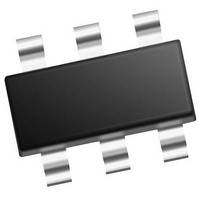
PIC10F322T-I/OT Microchip Technology, PIC10F322T-I/OT Datasheet - Page 72

PIC10F322T-I/OT
Manufacturer Part Number
PIC10F322T-I/OT
Description
896 B Flash, 64 B RAM, 4 I/O, 8bit ADC, PWM, CLC, DDS, CWG, TEMP Indicator, 2.3V
Manufacturer
Microchip Technology
Datasheet
1.PIC10F320-IOT.pdf
(210 pages)
Specifications of PIC10F322T-I/OT
Core
RISC
Processor Series
PIC10F
Data Bus Width
8 bit
Maximum Clock Frequency
31 KHz
Program Memory Size
512 B
Data Ram Size
64 B
Number Of Programmable I/os
4
Number Of Timers
2
Operating Temperature Range
- 40 C to + 85 C
Package / Case
SOT-23-6
Mounting Style
SMD/SMT
Maximum Operating Temperature
+ 85 C
Program Memory Type
Flash
Lead Free Status / Rohs Status
Details
Available stocks
Company
Part Number
Manufacturer
Quantity
Price
Company:
Part Number:
PIC10F322T-I/OT
Manufacturer:
VISHAY
Quantity:
11 490
Part Number:
PIC10F322T-I/OT
Manufacturer:
MICROCHIP/微芯
Quantity:
20 000
- Current page: 72 of 210
- Download datasheet (2Mb)
PIC10(L)F320/322
REGISTER 9-5:
DS41585A-page 72
bit 7
Legend:
R = Readable bit
S = Bit can only be set
‘1’ = Bit is set
bit 7
bit 6
bit 5
bit 4
bit 3
bit 2
bit 1
bit 0
Note 1:
U-1
—
2:
3:
(1)
Unimplemented bit, read as ‘1’.
The WRERR bit is automatically set by hardware when a program memory write or erase operation is started
(WR = 1).
The LWLO bit is ignored during a program memory erase operation (FREE = 1).
Unimplemented: Read as ‘1’
CFGS: Configuration Select bit
1 = Access Configuration, User ID and Device ID Registers
0 = Access Flash program memory
LWLO: Load Write Latches Only bit
1 = Only the addressed program memory write latch is loaded/updated on the next WR command
0 = The addressed program memory write latch is loaded/updated and a write of all program memory
FREE: Program Flash Erase Enable bit
1 = Performs an erase operation on the next WR command (hardware cleared upon completion)
0 = Performs an write operation on the next WR command
WRERR: Program/Erase Error Flag bit
1 = Condition indicates an improper program or erase sequence attempt or termination (bit is set
0 = The program or erase operation completed normally.
WREN: Program/Erase Enable bit
1 = Allows program/erase cycles
0 = Inhibits programming/erasing of program Flash
WR: Write Control bit
1 = Initiates a program Flash program/erase operation.
0 = Program/erase operation to the Flash is complete and inactive.
RD: Read Control bit
1 = Initiates a program Flash read. Read takes one cycle. RD is cleared in hardware. The RD bit can
0 = Does not initiate a program Flash read.
R/W-0/0
CFGS
write latches will be initiated on the next WR command
automatically on any set attempt (write ‘1’) of the WR bit).
The operation is self-timed and the bit is cleared by hardware once operation is complete.
The WR bit can only be set (not cleared) in software.
only be set (not cleared) in software.
PMCON1: PROGRAM MEMORY CONTROL 1 REGISTER
W = Writable bit
x = Bit is unknown
‘0’ = Bit is cleared
R/W-0/0
LWLO
R/W/HC-0/0 R/W/HC-0/q
FREE
Preliminary
(3)
U = Unimplemented bit, read as ‘0’
-n/n = Value at POR and BOR/Value at all other Resets
HC = Bit is cleared by hardware
WRERR
(2)
R/W-0/0
WREN
2011 Microchip Technology Inc.
R/S/HC-0/0
WR
R/S/HC-0/0
RD
bit 0
Related parts for PIC10F322T-I/OT
Image
Part Number
Description
Manufacturer
Datasheet
Request
R

Part Number:
Description:
896 B Flash, 64 B RAM, 4 I/O, 8bit ADC, PWM, CLC, DDS, CWG, TEMP Indicator, 2.3V
Manufacturer:
Microchip Technology

Part Number:
Description:
896 B Flash, 64 B RAM, 4 I/O, 8bit ADC, PWM, CLC, DDS, CWG, TEMP Indicator, 2.3V
Manufacturer:
Microchip Technology

Part Number:
Description:
896 B Flash, 64 B RAM, 4 I/O, 8bit ADC, PWM, CLC, DDS, CWG, TEMP Indicator, 2.3V
Manufacturer:
Microchip Technology

Part Number:
Description:
896 B Flash, 64 B RAM, 4 I/O, 8bit ADC, PWM, CLC, DDS, CWG, TEMP Indicator, 2.3V
Manufacturer:
Microchip Technology

Part Number:
Description:
896 B Flash, 64 B RAM, 4 I/O, 8bit ADC, PWM, CLC, DDS, CWG, TEMP Indicator, 2.3V
Manufacturer:
Microchip Technology

Part Number:
Description:
896 B Flash, 64 B RAM, 4 I/O, 8bit ADC, PWM, CLC, DDS, CWG, TEMP Indicator, 2.3V
Manufacturer:
Microchip Technology

Part Number:
Description:
384B Flash, 16B RAM, 4 I/O, 8bit ADC 6 SOT-23 BAG
Manufacturer:
Microchip Technology
Datasheet:

Part Number:
Description:
768B Flash, 23B RAM, 4 I/O, 8bit ADC 6 SOT-23 BAG
Manufacturer:
Microchip Technology
Datasheet:

Part Number:
Description:
384B Flash, 16B RAM, 4 I/O, 8bit ADC 6 SOT-23 BAG
Manufacturer:
Microchip Technology
Datasheet:

Part Number:
Description:
768B Flash, 23B RAM, 4 I/O, 8bit ADC 6 SOT-23 BAG
Manufacturer:
Microchip Technology
Datasheet:

Part Number:
Description:
PIC10F PROGRAMMER ADAPTER (SOT-23), PICKIT
Manufacturer:
Microchip Technology Inc.

Part Number:
Description:
Manufacturer:
Microchip Technology Inc.
Datasheet:

Part Number:
Description:
Manufacturer:
Microchip Technology Inc.
Datasheet:


