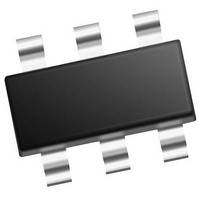
PIC10F322T-I/OT Microchip Technology, PIC10F322T-I/OT Datasheet - Page 75

PIC10F322T-I/OT
Manufacturer Part Number
PIC10F322T-I/OT
Description
896 B Flash, 64 B RAM, 4 I/O, 8bit ADC, PWM, CLC, DDS, CWG, TEMP Indicator, 2.3V
Manufacturer
Microchip Technology
Datasheet
1.PIC10F320-IOT.pdf
(210 pages)
Specifications of PIC10F322T-I/OT
Core
RISC
Processor Series
PIC10F
Data Bus Width
8 bit
Maximum Clock Frequency
31 KHz
Program Memory Size
512 B
Data Ram Size
64 B
Number Of Programmable I/os
4
Number Of Timers
2
Operating Temperature Range
- 40 C to + 85 C
Package / Case
SOT-23-6
Mounting Style
SMD/SMT
Maximum Operating Temperature
+ 85 C
Program Memory Type
Flash
Lead Free Status / Rohs Status
Details
Available stocks
Company
Part Number
Manufacturer
Quantity
Price
Company:
Part Number:
PIC10F322T-I/OT
Manufacturer:
VISHAY
Quantity:
11 490
Part Number:
PIC10F322T-I/OT
Manufacturer:
MICROCHIP/微芯
Quantity:
20 000
- Current page: 75 of 210
- Download datasheet (2Mb)
10.0
Depending on which peripherals are enabled, some or
all of the pins may not be available as general purpose
I/O. In general, when a peripheral is enabled on a port
pin, that pin cannot be used as a general purpose
output. However, the pin can still be read.
PORTA has three standard registers for its operation.
These registers are:
• TRISA register (data direction)
• PORTA register (reads the levels on the pins of
• LATA register (output latch)
Some ports may have one or more of the following
additional registers. These registers are:
• ANSELA (analog select)
• WPUA (weak pull-up)
The Data Latch (LATA register) is useful for read-
modify-write operations on the value that the I/O pins
are driving.
A write operation to the LATA register has the same
effect as a write to the corresponding PORTA register.
A read of the LATA register reads of the values held in
the I/O PORT latches, while a read of the PORTA
register reads the actual I/O pin value.
Ports that support analog inputs have an associated
ANSELA register. When an ANSEL bit is set, the digital
input buffer associated with that bit is disabled.
Disabling the input buffer prevents analog signal levels
on the pin between a logic high and low from causing
excessive current in the logic input circuitry. A
simplified model of a generic I/O port, without the
interfaces to other peripherals, is shown in
EXAMPLE 10-1:
2011 Microchip Technology Inc.
; This code example illustrates
; initializing the PORTA register. The
; other ports are initialized in the same
; manner.
BANKSEL
CLRF
BANKSEL
CLRF
BANKSEL
CLRF
BANKSEL
MOVLW
MOVWF
the device)
I/O PORT
PORTA
PORTA
LATA
LATA
ANSELA
ANSELA
TRISA
B'00000011'
TRISA
INITIALIZING PORTA
;not required on devices with 1 Bank of SFRs
;Init PORTA
;not required on devices with 1 Bank of SFRs
;
;not required on devices with 1 Bank of SFRs
;digital I/O
;not required on devices with 1 Bank of SFRs
;Set RA<1:0> as inputs
;and set RA<2:3> as
;outputs
Figure
10-1.
Preliminary
FIGURE 10-1:
To peripherals
Write PORTA
Write LATA
Data Bus
Read PORTA
PIC10(L)F320/322
Data Register
D
CK
Read LATA
ANSELA
I/O PORT OPERATION
Q
TRISA
DS41585A-page 75
V
V
DD
SS
I/O pin
Related parts for PIC10F322T-I/OT
Image
Part Number
Description
Manufacturer
Datasheet
Request
R

Part Number:
Description:
896 B Flash, 64 B RAM, 4 I/O, 8bit ADC, PWM, CLC, DDS, CWG, TEMP Indicator, 2.3V
Manufacturer:
Microchip Technology

Part Number:
Description:
896 B Flash, 64 B RAM, 4 I/O, 8bit ADC, PWM, CLC, DDS, CWG, TEMP Indicator, 2.3V
Manufacturer:
Microchip Technology

Part Number:
Description:
896 B Flash, 64 B RAM, 4 I/O, 8bit ADC, PWM, CLC, DDS, CWG, TEMP Indicator, 2.3V
Manufacturer:
Microchip Technology

Part Number:
Description:
896 B Flash, 64 B RAM, 4 I/O, 8bit ADC, PWM, CLC, DDS, CWG, TEMP Indicator, 2.3V
Manufacturer:
Microchip Technology

Part Number:
Description:
896 B Flash, 64 B RAM, 4 I/O, 8bit ADC, PWM, CLC, DDS, CWG, TEMP Indicator, 2.3V
Manufacturer:
Microchip Technology

Part Number:
Description:
896 B Flash, 64 B RAM, 4 I/O, 8bit ADC, PWM, CLC, DDS, CWG, TEMP Indicator, 2.3V
Manufacturer:
Microchip Technology

Part Number:
Description:
384B Flash, 16B RAM, 4 I/O, 8bit ADC 6 SOT-23 BAG
Manufacturer:
Microchip Technology
Datasheet:

Part Number:
Description:
768B Flash, 23B RAM, 4 I/O, 8bit ADC 6 SOT-23 BAG
Manufacturer:
Microchip Technology
Datasheet:

Part Number:
Description:
384B Flash, 16B RAM, 4 I/O, 8bit ADC 6 SOT-23 BAG
Manufacturer:
Microchip Technology
Datasheet:

Part Number:
Description:
768B Flash, 23B RAM, 4 I/O, 8bit ADC 6 SOT-23 BAG
Manufacturer:
Microchip Technology
Datasheet:

Part Number:
Description:
PIC10F PROGRAMMER ADAPTER (SOT-23), PICKIT
Manufacturer:
Microchip Technology Inc.

Part Number:
Description:
Manufacturer:
Microchip Technology Inc.
Datasheet:

Part Number:
Description:
Manufacturer:
Microchip Technology Inc.
Datasheet:


