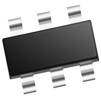
PIC10F322T-I/OT Microchip Technology, PIC10F322T-I/OT Datasheet - Page 63

PIC10F322T-I/OT
Manufacturer Part Number
PIC10F322T-I/OT
Description
896 B Flash, 64 B RAM, 4 I/O, 8bit ADC, PWM, CLC, DDS, CWG, TEMP Indicator, 2.3V
Manufacturer
Microchip Technology
Datasheet
1.PIC10F320-IOT.pdf
(210 pages)
Specifications of PIC10F322T-I/OT
Core
RISC
Processor Series
PIC10F
Data Bus Width
8 bit
Maximum Clock Frequency
31 KHz
Program Memory Size
512 B
Data Ram Size
64 B
Number Of Programmable I/os
4
Number Of Timers
2
Operating Temperature Range
- 40 C to + 85 C
Package / Case
SOT-23-6
Mounting Style
SMD/SMT
Maximum Operating Temperature
+ 85 C
Program Memory Type
Flash
Lead Free Status / Rohs Status
Details
Available stocks
Company
Part Number
Manufacturer
Quantity
Price
Company:
Part Number:
PIC10F322T-I/OT
Manufacturer:
VISHAY
Quantity:
11 490
Part Number:
PIC10F322T-I/OT
Manufacturer:
MICROCHIP/微芯
Quantity:
20 000
9.2.4
Program memory is programmed using the following
steps:
1.
2.
3.
4.
Before writing to program memory, the word(s) to be
written must be erased or previously unwritten. Pro-
gram memory can only be erased one row at a time. No
automatic erase occurs upon the initiation of the write.
Program memory can be written one or more words at
a time. The maximum number of words written at one
time is equal to the number of write latches. See
Figure 9-5
latches) for more details.
The write latches are aligned to the Flash row address
boundary
PMADRH:PMADRL, (PMADRH<6:0>:PMADRL<7:5>)
with the lower 5-bits of PMADRL, (PMADRL<4:0>)
determining the write latch being loaded. Write opera-
tions do not cross these boundaries. At the completion
of a program memory write operation, the data in the
write latches is reset to contain 0x3FFF.
2011 Microchip Technology Inc.
Load the address in PMADRH:PMADRL of the
row to be programmed.
Load each write latch with data.
Initiate a programming operation.
Repeat steps 1 through 3 until all data is written.
(row writes to program memory with 16 write
WRITING TO FLASH PROGRAM
MEMORY
defined
by
the
upper
10-bits
Preliminary
of
The following steps should be completed to load the
write latches and program a row of program memory.
These steps are divided into two parts. First, each write
latch is loaded with data from the PMDATH:PMDATL
using the unlock sequence with LWLO = 1. When the
last word to be loaded into the write latch is ready, the
LWLO bit is cleared and the unlock sequence
executed. This initiates the programming operation,
writing all the latches into Flash program memory.
1.
2.
3.
4.
5.
6.
7.
8.
9.
10. Load the PMDATH:PMDATL register pair with
11.
An example of the complete write sequence is shown in
Example
PMADRH:PMADRL register pair; the data is loaded
using indirect addressing.
Note:
Note:
Set the WREN bit of the PMCON1 register.
Clear the CFGS bit of the PMCON1 register.
Set the LWLO bit of the PMCON1 register.
When the LWLO bit of the PMCON1 register is
‘1’, the write sequence will only load the write
latches and will not initiate the write to Flash
program memory.
Load the PMADRH:PMADRL register pair with
the address of the location to be written.
Load the PMDATH:PMDATL register pair with
the program memory data to be written.
Execute the unlock sequence
“Flash Memory Unlock
latch is now loaded.
Increment the PMADRH:PMADRL register pair
to point to the next location.
Repeat steps 5 through 7 until all but the last
write latch has been loaded.
Clear the LWLO bit of the PMCON1 register.
When the LWLO bit of the PMCON1 register is
‘0’, the write sequence will initiate the write to
Flash program memory.
the program memory data to be written.
“Flash Memory Unlock
entire program memory latch content is now
written to Flash program memory.
Execute the unlock sequence
PIC10(L)F320/322
9-3. The initial address is loaded into the
The special unlock sequence is required
to load a write latch with data or initiate a
Flash programming operation. If the
unlock sequence is interrupted, writing to
the latches or program memory will not be
initiated.
The program memory write latches are
reset to the blank state (0x3FFF) at the
completion of every write or erase
operation. As a result, it is not necessary
to load all the program memory write
latches. Unloaded latches will remain in
the blank state.
Sequence”). The write
Sequence”). The
DS41585A-page 63
(Section 9.2.2
(Section 9.2.2


