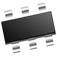
PIC10F322T-I/OT Microchip Technology, PIC10F322T-I/OT Datasheet - Page 76

PIC10F322T-I/OT
Manufacturer Part Number
PIC10F322T-I/OT
Description
896 B Flash, 64 B RAM, 4 I/O, 8bit ADC, PWM, CLC, DDS, CWG, TEMP Indicator, 2.3V
Manufacturer
Microchip Technology
Datasheet
1.PIC10F320-IOT.pdf
(210 pages)
Specifications of PIC10F322T-I/OT
Core
RISC
Processor Series
PIC10F
Data Bus Width
8 bit
Maximum Clock Frequency
31 KHz
Program Memory Size
512 B
Data Ram Size
64 B
Number Of Programmable I/os
4
Number Of Timers
2
Operating Temperature Range
- 40 C to + 85 C
Package / Case
SOT-23-6
Mounting Style
SMD/SMT
Maximum Operating Temperature
+ 85 C
Program Memory Type
Flash
Lead Free Status / Rohs Status
Details
Available stocks
Company
Part Number
Manufacturer
Quantity
Price
Company:
Part Number:
PIC10F322T-I/OT
Manufacturer:
VISHAY
Quantity:
11 490
Part Number:
PIC10F322T-I/OT
Manufacturer:
MICROCHIP/微芯
Quantity:
20 000
PIC10(L)F320/322
10.1
PORTA is a 8-bit wide, bidirectional port. The
corresponding data direction register is TRISA
(Register
corresponding PORTA pin an input (i.e., disable the
output driver). Clearing a TRISA bit (= 0) will make the
corresponding PORTA pin an output (i.e., enables
output driver and puts the contents of the output latch
on the selected pin).
initialize PORTA.
Reading the PORTA register
status of the pins, whereas writing to it will write to the
PORT latch. All write operations are read-modify-write
operations. Therefore, a write to a port implies that the
port pins are read, this value is modified and then
written to the PORT data latch (LATA).
The TRISA register
PORTA pin output drivers, even when they are being
used as analog inputs. The user should ensure the bits
in the TRISA register are maintained set when using
them as analog inputs. I/O pins configured as analog
input always read ‘0’.
10.1.1
Each of the PORTA pins has an individually configu-
rable internal weak pull-up. Control bits WPUA<3:0>
enable or disable each pull-up (see
Each weak pull-up is automatically turned off when the
port pin is configured as an output. All pull-ups are dis-
abled on a Power-on Reset by the WPUEN bit of the
OPTION_REG register.
10.1.2
The ANSELA register
configure the Input mode of an I/O pin to analog.
Setting the appropriate ANSELA bit high will cause all
digital reads on the pin to be read as ‘0’ and allow
analog functions on the pin to operate correctly.
The state of the ANSELA bits has no effect on digital
output functions. A pin with TRIS clear and ANSEL set
will still operate as a digital output, but the Input mode
will be analog. This can cause unexpected behavior
when executing read-modify-write instructions on the
affected port.
DS41585A-page 76
Note:
PORTA Registers
10-2). Setting a TRISA bit (= 1) will make the
WEAK PULL-UPS
ANSELA REGISTER
The ANSELA bits default to the Analog
mode after Reset. To use any pins as
digital general purpose or peripheral
inputs, the corresponding ANSEL bits
must be initialized to ‘0’ by user software.
Example 10-1
(Register
(Register
(Register
10-2) controls the
10-4) is used to
10-1) reads the
shows how to
Register
10-5).
Preliminary
10.1.3
Each PORTA pin is multiplexed with other functions. The
pins, their combined functions and their output priorities
are shown in
When multiple outputs are enabled, the actual pin
control goes to the peripheral with the highest priority.
Digital output functions may control the pin when it is in
Analog mode with the priority shown in
TABLE 10-1:
Note 1:
Pin Name
RA0
RA1
RA2
RA3
Priority listed from highest to lowest.
PORTA FUNCTIONS AND OUTPUT
PRIORITIES
Table
PORTA OUTPUT PRIORITY
10-1.
2011 Microchip Technology Inc.
Function Priority
ICSPDAT
CWG1A
PWM1
RA0
CWG1B
PWM2
CLC1
RA1
NCO1
CLKR
RA2
None
Table
10-1.
(1)


