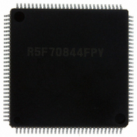
DF70844AD80FPV Renesas Electronics America, DF70844AD80FPV Datasheet - Page 265

DF70844AD80FPV
Manufacturer Part Number
DF70844AD80FPV
Description
IC SUPERH MCU FLASH 112LQFP
Manufacturer
Renesas Electronics America
Series
SuperH® SH7080r
Datasheet
1.DF70844AD80FPV.pdf
(1644 pages)
Specifications of DF70844AD80FPV
Core Size
32-Bit
Program Memory Size
256KB (256K x 8)
Core Processor
SH-2
Speed
80MHz
Connectivity
EBI/EMI, FIFO, I²C, SCI, SSU
Peripherals
DMA, POR, PWM, WDT
Number Of I /o
76
Program Memory Type
FLASH
Ram Size
16K x 8
Voltage - Supply (vcc/vdd)
3 V ~ 5.5 V
Data Converters
A/D 8x10b
Oscillator Type
Internal
Operating Temperature
-40°C ~ 85°C
Package / Case
112-LQFP
No. Of I/o's
76
Ram Memory Size
16KB
Cpu Speed
80MHz
Digital Ic Case Style
LQFP
Supply Voltage Range
3V To 3.6V, 4.5V To 5.5V
Embedded Interface Type
I2C, SCI
Rohs Compliant
Yes
Lead Free Status / RoHS Status
Lead free / RoHS Compliant
For Use With
R0K570865S001BE - KIT STARTER FOR SH7086R0K570865S000BE - KIT STARTER FOR SH7086HS0005KCU11H - EMULATOR E10A-USB H8S(X),SH2(A)
Eeprom Size
-
Lead Free Status / RoHS Status
Lead free / RoHS Compliant, Lead free / RoHS Compliant
Available stocks
Company
Part Number
Manufacturer
Quantity
Price
Company:
Part Number:
DF70844AD80FPV
Manufacturer:
Renesas Electronics America
Quantity:
10 000
- Current page: 265 of 1644
- Download datasheet (10Mb)
Table 8.11 DTC Bus Release Timing
Notes: 1. The bus mastership is only released for the external space access request from the
Setting
Setting 1
Setting 2
Setting 3
Setting 4*
Setting 5
2
2. There are following restrictions in setting 4.
3. Don't care.
DTLOCK CSSTP1
1
0
0
0
1
CPU after a vector read.
Bus Function Extending Register (BSCEHR)
•
•
•
•
0
0
1
1
1
Clock setting by the frequency control register (FRQCR) must be
Iφ:Bφ:Pφ:MIφ:MPφ = 8:4:4:4:4, 4:2:2:2:2, or 2:1:1:1:1.
Locate vector information in on-chip ROM or on-chip RAM.
Locate transfer information in on-chip RAM.
Transfer is allowed between on-chip RAM and on-chip peripheral module or
between external memory and on-chip peripheral module.
CSSTP2
*
0
*
*
*
Setting
3
3
3
3
CSSTP3
1
*
*
*
1
3
3
3
DTBST
0
0
0
1
0
After
vector
read
O
x
x
x
O
NOP cycle
generation*
O
O
x
x
x
(O: Bus is released; x: Bus is not released)
Rev. 3.00 May 17, 2007 Page 207 of 1582
Section 8 Data Transfer Controller (DTC)
1
After
transfer
information
read
O
x
x
x
O
Bus Release Timing
After a
single
data
transfer
O
x
x
x
O
REJ09B0181-0300
After write-back of
transfer information
Normal
transfer
O
O
O
O
O
Continuous
transfer
O
O
O
x
O
Related parts for DF70844AD80FPV
Image
Part Number
Description
Manufacturer
Datasheet
Request
R

Part Number:
Description:
KIT STARTER FOR M16C/29
Manufacturer:
Renesas Electronics America
Datasheet:

Part Number:
Description:
KIT STARTER FOR R8C/2D
Manufacturer:
Renesas Electronics America
Datasheet:

Part Number:
Description:
R0K33062P STARTER KIT
Manufacturer:
Renesas Electronics America
Datasheet:

Part Number:
Description:
KIT STARTER FOR R8C/23 E8A
Manufacturer:
Renesas Electronics America
Datasheet:

Part Number:
Description:
KIT STARTER FOR R8C/25
Manufacturer:
Renesas Electronics America
Datasheet:

Part Number:
Description:
KIT STARTER H8S2456 SHARPE DSPLY
Manufacturer:
Renesas Electronics America
Datasheet:

Part Number:
Description:
KIT STARTER FOR R8C38C
Manufacturer:
Renesas Electronics America
Datasheet:

Part Number:
Description:
KIT STARTER FOR R8C35C
Manufacturer:
Renesas Electronics America
Datasheet:

Part Number:
Description:
KIT STARTER FOR R8CL3AC+LCD APPS
Manufacturer:
Renesas Electronics America
Datasheet:

Part Number:
Description:
KIT STARTER FOR RX610
Manufacturer:
Renesas Electronics America
Datasheet:

Part Number:
Description:
KIT STARTER FOR R32C/118
Manufacturer:
Renesas Electronics America
Datasheet:

Part Number:
Description:
KIT DEV RSK-R8C/26-29
Manufacturer:
Renesas Electronics America
Datasheet:

Part Number:
Description:
KIT STARTER FOR SH7124
Manufacturer:
Renesas Electronics America
Datasheet:

Part Number:
Description:
KIT STARTER FOR H8SX/1622
Manufacturer:
Renesas Electronics America
Datasheet:

Part Number:
Description:
KIT DEV FOR SH7203
Manufacturer:
Renesas Electronics America
Datasheet:


