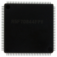
DF70844AD80FPV Renesas Electronics America, DF70844AD80FPV Datasheet - Page 61

DF70844AD80FPV
Manufacturer Part Number
DF70844AD80FPV
Description
IC SUPERH MCU FLASH 112LQFP
Manufacturer
Renesas Electronics America
Series
SuperH® SH7080r
Datasheet
1.DF70844AD80FPV.pdf
(1644 pages)
Specifications of DF70844AD80FPV
Core Size
32-Bit
Program Memory Size
256KB (256K x 8)
Core Processor
SH-2
Speed
80MHz
Connectivity
EBI/EMI, FIFO, I²C, SCI, SSU
Peripherals
DMA, POR, PWM, WDT
Number Of I /o
76
Program Memory Type
FLASH
Ram Size
16K x 8
Voltage - Supply (vcc/vdd)
3 V ~ 5.5 V
Data Converters
A/D 8x10b
Oscillator Type
Internal
Operating Temperature
-40°C ~ 85°C
Package / Case
112-LQFP
No. Of I/o's
76
Ram Memory Size
16KB
Cpu Speed
80MHz
Digital Ic Case Style
LQFP
Supply Voltage Range
3V To 3.6V, 4.5V To 5.5V
Embedded Interface Type
I2C, SCI
Rohs Compliant
Yes
Lead Free Status / RoHS Status
Lead free / RoHS Compliant
For Use With
R0K570865S001BE - KIT STARTER FOR SH7086R0K570865S000BE - KIT STARTER FOR SH7086HS0005KCU11H - EMULATOR E10A-USB H8S(X),SH2(A)
Eeprom Size
-
Lead Free Status / RoHS Status
Lead free / RoHS Compliant, Lead free / RoHS Compliant
Available stocks
Company
Part Number
Manufacturer
Quantity
Price
Company:
Part Number:
DF70844AD80FPV
Manufacturer:
Renesas Electronics America
Quantity:
10 000
- Current page: 61 of 1644
- Download datasheet (10Mb)
Items
On-chip RAM
Bus state controller
(BSC)
Direct memory access
controller (DMAC)
Data transfer
controller (DTC)
Specification
•
•
•
•
•
•
•
•
•
•
•
•
•
•
•
•
•
16 kbytes or 32 kbytes
Address space divided into nine areas: Eight areas (CS0 to CS7), each
a maximum of 64 Mbytes, and one area (CS8) of a maximum of 1
Gbytes (a total of three areas in SH7083, eight areas in
SH7084/SH7085, and nine areas in SH7086)
8-bit external bus
16-bit external bus
32-bit external bus (only in SH7085/SH7086)
The following features settable for each area independently
Bus size (8, 16, or 32 bits)
Number of access wait cycles
Idle wait cycle insertion
Specifying the memory to be connected to each area enables direct
Outputs a chip select signal according to the target area
Four channels
External request available
Burst mode and cycle steal mode
Data transfer activated by an on-chip peripheral module interrupt can
be done independently of the CPU transfer.
Transfer mode selectable for each interrupt source (transfer mode is
specified in memory)
Multiple data transfer enabled for one activation source
Various transfer modes
Normal mode, repeat mode, or block transfer mode can be selected.
Data transfer size can be specified as byte, word, or longword
The interrupt that activated the DTC can be issued to the CPU.
A CPU interrupt can be requested after one data transfer completion.
A CPU interrupt can be requested after all specified data transfer
completion.
connection to SRAM, SRAM with byte selection, burst ROM (clock
synchronous or asynchronous), MPX-I/O, burst MPX-I/O, SDRAM,
and PCMCIA
Rev. 3.00 May 17, 2007 Page 3 of 1582
Section 1 Overview
REJ09B0181-0300
Related parts for DF70844AD80FPV
Image
Part Number
Description
Manufacturer
Datasheet
Request
R

Part Number:
Description:
KIT STARTER FOR M16C/29
Manufacturer:
Renesas Electronics America
Datasheet:

Part Number:
Description:
KIT STARTER FOR R8C/2D
Manufacturer:
Renesas Electronics America
Datasheet:

Part Number:
Description:
R0K33062P STARTER KIT
Manufacturer:
Renesas Electronics America
Datasheet:

Part Number:
Description:
KIT STARTER FOR R8C/23 E8A
Manufacturer:
Renesas Electronics America
Datasheet:

Part Number:
Description:
KIT STARTER FOR R8C/25
Manufacturer:
Renesas Electronics America
Datasheet:

Part Number:
Description:
KIT STARTER H8S2456 SHARPE DSPLY
Manufacturer:
Renesas Electronics America
Datasheet:

Part Number:
Description:
KIT STARTER FOR R8C38C
Manufacturer:
Renesas Electronics America
Datasheet:

Part Number:
Description:
KIT STARTER FOR R8C35C
Manufacturer:
Renesas Electronics America
Datasheet:

Part Number:
Description:
KIT STARTER FOR R8CL3AC+LCD APPS
Manufacturer:
Renesas Electronics America
Datasheet:

Part Number:
Description:
KIT STARTER FOR RX610
Manufacturer:
Renesas Electronics America
Datasheet:

Part Number:
Description:
KIT STARTER FOR R32C/118
Manufacturer:
Renesas Electronics America
Datasheet:

Part Number:
Description:
KIT DEV RSK-R8C/26-29
Manufacturer:
Renesas Electronics America
Datasheet:

Part Number:
Description:
KIT STARTER FOR SH7124
Manufacturer:
Renesas Electronics America
Datasheet:

Part Number:
Description:
KIT STARTER FOR H8SX/1622
Manufacturer:
Renesas Electronics America
Datasheet:

Part Number:
Description:
KIT DEV FOR SH7203
Manufacturer:
Renesas Electronics America
Datasheet:


