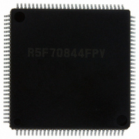
DF70844AD80FPV Renesas Electronics America, DF70844AD80FPV Datasheet - Page 689

DF70844AD80FPV
Manufacturer Part Number
DF70844AD80FPV
Description
IC SUPERH MCU FLASH 112LQFP
Manufacturer
Renesas Electronics America
Series
SuperH® SH7080r
Datasheet
1.DF70844AD80FPV.pdf
(1644 pages)
Specifications of DF70844AD80FPV
Core Size
32-Bit
Program Memory Size
256KB (256K x 8)
Core Processor
SH-2
Speed
80MHz
Connectivity
EBI/EMI, FIFO, I²C, SCI, SSU
Peripherals
DMA, POR, PWM, WDT
Number Of I /o
76
Program Memory Type
FLASH
Ram Size
16K x 8
Voltage - Supply (vcc/vdd)
3 V ~ 5.5 V
Data Converters
A/D 8x10b
Oscillator Type
Internal
Operating Temperature
-40°C ~ 85°C
Package / Case
112-LQFP
No. Of I/o's
76
Ram Memory Size
16KB
Cpu Speed
80MHz
Digital Ic Case Style
LQFP
Supply Voltage Range
3V To 3.6V, 4.5V To 5.5V
Embedded Interface Type
I2C, SCI
Rohs Compliant
Yes
Lead Free Status / RoHS Status
Lead free / RoHS Compliant
For Use With
R0K570865S001BE - KIT STARTER FOR SH7086R0K570865S000BE - KIT STARTER FOR SH7086HS0005KCU11H - EMULATOR E10A-USB H8S(X),SH2(A)
Eeprom Size
-
Lead Free Status / RoHS Status
Lead free / RoHS Compliant, Lead free / RoHS Compliant
Available stocks
Company
Part Number
Manufacturer
Quantity
Price
Company:
Part Number:
DF70844AD80FPV
Manufacturer:
Renesas Electronics America
Quantity:
10 000
- Current page: 689 of 1644
- Download datasheet (10Mb)
11.7.11 Contention between Buffer Register Write and Input Capture
If an input capture signal is generated in the T2 state of a buffer register write cycle, the buffer
operation takes precedence and the write to the buffer register is not performed.
Figure 11.130 shows the timing in this case.
11.7.12 TCNT_2 Write and Overflow/Underflow Contention in Cascade Connection
With timer counters TCNT_1 and TCNT_2 in a cascade connection, when a contention occurs
during TCNT_1 count (during a TCNT_2 overflow/underflow) in the T2 state of the TCNT_2
write cycle, the write to TCNT_2 is conducted, and the TCNT_1 count signal is disabled. At this
point, if there is match with TGRA_1 and the TCNT_1 value, a compare signal is issued.
Furthermore, when the TCNT_1 count clock is selected as the input capture source of channel 0,
TGRA_0 to TGRD_0 carry out the input capture operation. In addition, when the compare
match/input capture is selected as the input capture source of TGRB_1, TGRB_1 carries out input
capture operation. The timing is shown in figure 11.131.
For cascade connections, be sure to synchronize settings for channels 1 and 2 when setting TCNT
clearing.
Figure 11.130 Contention between Buffer Register Write and Input Capture
MPφ
Address
Write signal
Input capture
signal
TCNT
TGR
Buffer register
Buffer register write cycle
M
Buffer register
T1
address
Section 11 Multi-Function Timer Pulse Unit 2 (MTU2)
N
T2
Rev. 3.00 May 17, 2007 Page 631 of 1582
M
N
REJ09B0181-0300
Related parts for DF70844AD80FPV
Image
Part Number
Description
Manufacturer
Datasheet
Request
R

Part Number:
Description:
KIT STARTER FOR M16C/29
Manufacturer:
Renesas Electronics America
Datasheet:

Part Number:
Description:
KIT STARTER FOR R8C/2D
Manufacturer:
Renesas Electronics America
Datasheet:

Part Number:
Description:
R0K33062P STARTER KIT
Manufacturer:
Renesas Electronics America
Datasheet:

Part Number:
Description:
KIT STARTER FOR R8C/23 E8A
Manufacturer:
Renesas Electronics America
Datasheet:

Part Number:
Description:
KIT STARTER FOR R8C/25
Manufacturer:
Renesas Electronics America
Datasheet:

Part Number:
Description:
KIT STARTER H8S2456 SHARPE DSPLY
Manufacturer:
Renesas Electronics America
Datasheet:

Part Number:
Description:
KIT STARTER FOR R8C38C
Manufacturer:
Renesas Electronics America
Datasheet:

Part Number:
Description:
KIT STARTER FOR R8C35C
Manufacturer:
Renesas Electronics America
Datasheet:

Part Number:
Description:
KIT STARTER FOR R8CL3AC+LCD APPS
Manufacturer:
Renesas Electronics America
Datasheet:

Part Number:
Description:
KIT STARTER FOR RX610
Manufacturer:
Renesas Electronics America
Datasheet:

Part Number:
Description:
KIT STARTER FOR R32C/118
Manufacturer:
Renesas Electronics America
Datasheet:

Part Number:
Description:
KIT DEV RSK-R8C/26-29
Manufacturer:
Renesas Electronics America
Datasheet:

Part Number:
Description:
KIT STARTER FOR SH7124
Manufacturer:
Renesas Electronics America
Datasheet:

Part Number:
Description:
KIT STARTER FOR H8SX/1622
Manufacturer:
Renesas Electronics America
Datasheet:

Part Number:
Description:
KIT DEV FOR SH7203
Manufacturer:
Renesas Electronics America
Datasheet:


