Z8F042AHH020EG Zilog, Z8F042AHH020EG Datasheet - Page 93
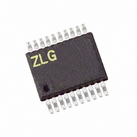
Z8F042AHH020EG
Manufacturer Part Number
Z8F042AHH020EG
Description
IC ENCORE XP MCU FLASH 4K 20SSOP
Manufacturer
Zilog
Series
Encore!® XP®r
Datasheet
1.Z8F08200100KIT.pdf
(264 pages)
Specifications of Z8F042AHH020EG
Core Processor
Z8
Core Size
8-Bit
Speed
20MHz
Connectivity
IrDA, UART/USART
Peripherals
Brown-out Detect/Reset, LED, LVD, POR, PWM, Temp Sensor, WDT
Number Of I /o
17
Program Memory Size
4KB (4K x 8)
Program Memory Type
FLASH
Eeprom Size
128 x 8
Ram Size
1K x 8
Voltage - Supply (vcc/vdd)
2.7 V ~ 3.6 V
Data Converters
A/D 7x10b
Oscillator Type
Internal
Operating Temperature
-40°C ~ 105°C
Package / Case
20-SSOP
Lead Free Status / RoHS Status
Lead free / RoHS Compliant
Other names
269-4156
Z8F042AHH020EG
Z8F042AHH020EG


Table 43. Timer 0–1 PWM High Byte Register (TxPWMH)
Table 44. Timer 0–1 PWM Low Byte Register (TxPWML)
Table 45. Timer 0–3 Control 0 Register (TxCTL0)
PS022517-0508
BITS
FIELD
RESET
R/W
ADDR
BITS
FIELD
RESET
R/W
ADDR
BITS
FIELD
RESET
R/W
ADDR
Timer 0–3 Control 0 Registers
7
7
7
PWMH and PWML—Pulse-Width Modulator High and Low Bytes
These two bytes, {PWMH[7:0], PWML[7:0]}, form a 16-bit value that is compared to the
current 16-bit timer count. When a match occurs, the PWM output changes state. The
PWM output value is set by the TPOL bit in the Timer Control Register (TxCTL) register.
The TxPWMH and TxPWML registers also store the 16-bit captured timer value when
operating in CAPTURE or CAPTURE/COMPARE modes.
The Timer 0–3 Control 0 (TxCTL0) registers
CSC—Cascade Timers
0 = Timer Input signal comes from the pin.
1 = For Timer 0, input signal is connected to Timer 1 output.
For Timer 1, input signal is connected to Timer 0 output.
6
Reserved
6
6
5
5
5
F06H, F0EH, F16H, F1EH
4
CSC
4
4
F04H, F0CH
F05H, F0DH
PWMH
PWML
R/W
R/W
R/W
0
0
0
3
(Table
3
3
45) allow cascading of the Timers.
2
Z8 Encore! XP
2
2
Reserved
Product Specification
1
1
1
®
F0822 Series
0
0
0
Timers
80
Related parts for Z8F042AHH020EG
Image
Part Number
Description
Manufacturer
Datasheet
Request
R

Part Number:
Description:
Communication Controllers, ZILOG INTELLIGENT PERIPHERAL CONTROLLER (ZIP)
Manufacturer:
Zilog, Inc.
Datasheet:

Part Number:
Description:
KIT DEV FOR Z8 ENCORE 16K TO 64K
Manufacturer:
Zilog
Datasheet:

Part Number:
Description:
KIT DEV Z8 ENCORE XP 28-PIN
Manufacturer:
Zilog
Datasheet:

Part Number:
Description:
DEV KIT FOR Z8 ENCORE 8K/4K
Manufacturer:
Zilog
Datasheet:

Part Number:
Description:
KIT DEV Z8 ENCORE XP 28-PIN
Manufacturer:
Zilog
Datasheet:

Part Number:
Description:
DEV KIT FOR Z8 ENCORE 4K TO 8K
Manufacturer:
Zilog
Datasheet:
Part Number:
Description:
CMOS Z8 microcontroller. ROM 16 Kbytes, RAM 256 bytes, speed 16 MHz, 32 lines I/O, 3.0V to 5.5V
Manufacturer:
Zilog, Inc.
Datasheet:
Part Number:
Description:
Low-cost microcontroller. 512 bytes ROM, 61 bytes RAM, 8 MHz
Manufacturer:
Zilog, Inc.
Datasheet:
Part Number:
Description:
Z8 4K OTP Microcontroller
Manufacturer:
Zilog, Inc.
Datasheet:
Part Number:
Description:
CMOS SUPER8 ROMLESS MCU
Manufacturer:
Zilog, Inc.
Datasheet:
Part Number:
Description:
SL1866 CMOSZ8 OTP Microcontroller
Manufacturer:
Zilog, Inc.
Datasheet:
Part Number:
Description:
SL1866 CMOSZ8 OTP Microcontroller
Manufacturer:
Zilog, Inc.
Datasheet:
Part Number:
Description:
OTP (KB) = 1, RAM = 125, Speed = 12, I/O = 14, 8-bit Timers = 2, Comm Interfaces Other Features = Por, LV Protect, Voltage = 4.5-5.5V
Manufacturer:
Zilog, Inc.
Datasheet:
Part Number:
Description:
Manufacturer:
Zilog, Inc.
Datasheet: