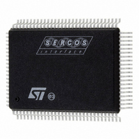
ST92F150JDV1QC STMicroelectronics, ST92F150JDV1QC Datasheet - Page 211

ST92F150JDV1QC
Manufacturer Part Number
ST92F150JDV1QC
Description
IC MCU 128K FLASH 100-PQFP
Manufacturer
STMicroelectronics
Series
ST9r
Datasheet
1.ST92F150CV1TB.pdf
(429 pages)
Specifications of ST92F150JDV1QC
Core Processor
ST9
Core Size
8/16-Bit
Speed
24MHz
Connectivity
CAN, I²C, LIN, SCI, SPI
Peripherals
DMA, LVD, POR, PWM, WDT
Number Of I /o
77
Program Memory Size
128KB (128K x 8)
Program Memory Type
FLASH
Eeprom Size
1K x 8
Ram Size
6K x 8
Voltage - Supply (vcc/vdd)
4.5 V ~ 5.5 V
Data Converters
A/D 16x10b
Oscillator Type
Internal
Operating Temperature
-40°C ~ 125°C
Package / Case
100-QFP
Processor Series
ST92F15x
Core
ST9
Data Bus Width
8 bit, 16 bit
Data Ram Size
6 KB
Interface Type
CAN, I2C, SCI, SPI
Maximum Clock Frequency
24 MHz
Number Of Programmable I/os
80
Number Of Timers
5 x 16 bit
Operating Supply Voltage
4.5 V to 5.5 V
Maximum Operating Temperature
+ 105 C
Mounting Style
SMD/SMT
Development Tools By Supplier
ST92F150-EPB
Minimum Operating Temperature
- 40 C
On-chip Adc
16 bit x 10 bit
Case
QFP
Lead Free Status / RoHS Status
Lead free / RoHS Compliant
Other names
497-2137
Available stocks
Company
Part Number
Manufacturer
Quantity
Price
- Current page: 211 of 429
- Download datasheet (8Mb)
MULTIFUNCTION TIMER (Cont’d)
INTERRUPT/DMA CONTROL REGISTER
(IDCR)
R243 - Read/Write
Register Page: 9
Reset value: 1100 0111 (C7h)
Bit 7 = CPE: Capture 0 EOB.
This bit is set by hardware when the End Of Block
condition is reached during a Capture 0 DMA op-
eration with the Swap mode enabled. When Swap
mode is disabled (SWEN bit = “0”), the CPE bit is
forced to 1 by hardware.
0: No end of block condition
1: Capture 0 End of block
Bit 6 = CME: Compare 0 EOB.
This bit is set by hardware when the End Of Block
condition is reached during a Compare 0 DMA op-
eration with the Swap mode enabled. When the
Swap mode is disabled (SWEN bit = “0”), the CME
bit is forced to 1 by hardware.
0: No end of block condition
1: Compare 0 End of block
Bit 5 = DCTS: DMA capture transfer source.
This bit is set and cleared by software. It selects
the source of the DMA operation related to the
channel associated with the Capture 0.
Note: The I/O port source is available only on spe-
cific devices.
0: REG0R register
1: I/O port.
Bit 4 = DCTD: DMA compare transfer destination.
This bit is set and cleared by software. It selects
the destination of the DMA operation related to the
channel associated with Compare 0.
Note: The I/O port destination is available only on
specific devices.
0: CMP0R register
1: I/O port
CPE CME DCTS DCTD SWEN PL2 PL1 PL0
7
0
Bit 3 = SWEN: Swap function enable.
This bit is set and cleared by software.
0: Disable Swap mode
1: Enable Swap mode for both DMA channels.
Bits 2:0 = PL[2:0]: Interrupt/DMA priority level.
With these three bits it is possible to select the In-
terrupt and DMA priority level of each timer, as one
of eight levels (see Interrupt/DMA chapter).
I/O CONNECTION REGISTER (IOCR)
R248 - Read/Write
Register Page: 9
Reset value: 1111 1100 (FCh)
Bits 7:2 = not used.
Bit 1 = SC1: Select connection odd.
This bit is set and cleared by software. It selects if
the TxOUTA and TxINA pins for Timer 1 and Timer
3 are connected on-chip or not.
0: T1OUTA / T1INA and T3OUTA/ T3INA uncon-
1: T1OUTA connected internally to T1INA and
Bit 0 = SC0: Select connection even.
This bit is set and cleared by software. It selects if
the TxOUTA and TxINA pins for Timer 0 and Timer
2 are connected on-chip or not.
0: T0OUTA / T0INA and T2OUTA/ T2INA uncon-
1: T0OUTA connected internally to T0INA and
Note: Timer 1 and 2 are available only on some
devices. Refer to the device block diagram and
register map.
nected
T3OUTA connected internally to T3INA
nected
T2OUTA connected internally to T2INA
7
MULTIFUNCTION TIMER (MFT)
SC1
211/429
SC0
0
9
Related parts for ST92F150JDV1QC
Image
Part Number
Description
Manufacturer
Datasheet
Request
R

Part Number:
Description:
BOARD PROGRAM FOR ST92F150 MCU
Manufacturer:
STMicroelectronics
Datasheet:

Part Number:
Description:
BOARD EVALUATION FOR ST9 SERIES
Manufacturer:
STMicroelectronics
Datasheet:

Part Number:
Description:
BOARD EMULATOR FOR ST9 SERIES
Manufacturer:
STMicroelectronics
Datasheet:

Part Number:
Description:
MCU, MPU & DSP Development Tools ST9 Dedication Board
Manufacturer:
STMicroelectronics
Datasheet:

Part Number:
Description:
STMicroelectronics [RIPPLE-CARRY BINARY COUNTER/DIVIDERS]
Manufacturer:
STMicroelectronics
Datasheet:

Part Number:
Description:
STMicroelectronics [LIQUID-CRYSTAL DISPLAY DRIVERS]
Manufacturer:
STMicroelectronics
Datasheet:

Part Number:
Description:
BOARD EVAL FOR MEMS SENSORS
Manufacturer:
STMicroelectronics
Datasheet:

Part Number:
Description:
NPN TRANSISTOR POWER MODULE
Manufacturer:
STMicroelectronics
Datasheet:

Part Number:
Description:
TURBOSWITCH ULTRA-FAST HIGH VOLTAGE DIODE
Manufacturer:
STMicroelectronics
Datasheet:

Part Number:
Description:
Manufacturer:
STMicroelectronics
Datasheet:

Part Number:
Description:
DIODE / SCR MODULE
Manufacturer:
STMicroelectronics
Datasheet:

Part Number:
Description:
DIODE / SCR MODULE
Manufacturer:
STMicroelectronics
Datasheet:


