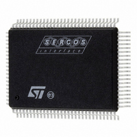
ST92F150JDV1QC STMicroelectronics, ST92F150JDV1QC Datasheet - Page 271

ST92F150JDV1QC
Manufacturer Part Number
ST92F150JDV1QC
Description
IC MCU 128K FLASH 100-PQFP
Manufacturer
STMicroelectronics
Series
ST9r
Datasheet
1.ST92F150CV1TB.pdf
(429 pages)
Specifications of ST92F150JDV1QC
Core Processor
ST9
Core Size
8/16-Bit
Speed
24MHz
Connectivity
CAN, I²C, LIN, SCI, SPI
Peripherals
DMA, LVD, POR, PWM, WDT
Number Of I /o
77
Program Memory Size
128KB (128K x 8)
Program Memory Type
FLASH
Eeprom Size
1K x 8
Ram Size
6K x 8
Voltage - Supply (vcc/vdd)
4.5 V ~ 5.5 V
Data Converters
A/D 16x10b
Oscillator Type
Internal
Operating Temperature
-40°C ~ 125°C
Package / Case
100-QFP
Processor Series
ST92F15x
Core
ST9
Data Bus Width
8 bit, 16 bit
Data Ram Size
6 KB
Interface Type
CAN, I2C, SCI, SPI
Maximum Clock Frequency
24 MHz
Number Of Programmable I/os
80
Number Of Timers
5 x 16 bit
Operating Supply Voltage
4.5 V to 5.5 V
Maximum Operating Temperature
+ 105 C
Mounting Style
SMD/SMT
Development Tools By Supplier
ST92F150-EPB
Minimum Operating Temperature
- 40 C
On-chip Adc
16 bit x 10 bit
Case
QFP
Lead Free Status / RoHS Status
Lead free / RoHS Compliant
Other names
497-2137
Available stocks
Company
Part Number
Manufacturer
Quantity
Price
- Current page: 271 of 429
- Download datasheet (8Mb)
I
Note: Until the pending bit is reset (while the cor-
responding mask bit is set), the peripheral proc-
esses an interrupt request. So, if at the end of an
interrupt routine the pending bit is not reset, anoth-
er interrupt request is performed.
Note: Before the end of the transmission and re-
ception interrupt routines, the I2CSR1.BTF flag bit
should be checked, to acknowledge any interrupt
requests that occurred during the interrupt routine
and to avoid masking subsequent interrupt re-
quests.
Note: The “Error” event interrupt pending bit
(I2CISR.IERRP) is forced high when the error
event flags are set (ADD10, ADSL and SB flags of
the I2CSR1 register; SCLF, ADDTX, AF, STOPF,
ARLO and BERR flags of the I2CSR2 register).
Moreover the Transmitting End Of Block interrupt
has the same priority as the “Peripheral Ready to
Transmit” interrupt and the Receiving End Of
Block interrupt has the same priority as the “Data
received” interrupt.
10.8.6 DMA Features
The peripheral can use the ST9+ on-chip Direct
Memory Access (DMA) channels to provide high-
speed data transaction between the peripheral
and contiguous locations of Register File, and
Memory. The transactions can occur from and to-
ward the peripheral. The maximum number of
transactions that each DMA channel can perform
is 222 if the register file is selected or 65536 if
memory is selected. The control of the DMA fea-
tures is performed using registers placed in the pe-
ripheral
I2CRDAP, I2CRDC, I2CTDAP, I2CTDC).
Each DMA transfer consists of three operations:
– A load from/to the peripheral data register
2
C BUS INTERFACE (Cont’d)
(I2CDR) to/from a location of Register File/Mem-
register
page
(I2CISR,
I2CIMR,
– A post-increment of the DMA Address Register
– A post-decrement of the DMA transaction coun-
The priority level of the DMA features of the I
interface with respect to the other peripherals and
the CPU is the same as programmed in the
I2CISR register for the interrupt sources. In the in-
ternal priority level order of the peripheral, the “Er-
ror” interrupt sources have higher priority, followed
by DMA, “Data received” and “Receiving End Of
Block” interrupts, “Peripheral Ready to Transmit”
and “Transmitting End Of Block”.
Refer to the Interrupt and DMA chapters for details
on the priority levels.
The DMA features are enabled by setting the cor-
responding enabling bits (RXDM, TXDM) in the
I2CIMR register. It is possible to select also the di-
rection of the DMA transactions.
Once the DMA transfer is completed (the transac-
tion counter reaches 0 value), an interrupt request
to the CPU is generated. This kind of interrupt is
called “End Of Block”. The peripheral sends two
different “End Of Block” interrupts depending on
the direction of the DMA (Receiving End Of Block -
Transmitting End Of Block). These interrupt
sources have dedicated interrupt pending bits in
the I2CIMR register (REOBP, TEOBP) and they
are mapped on the same interrupt vectors as re-
spectively “Data Received” and “Peripheral Ready
to Transmit” interrupt sources. The same corre-
spondence exists about the internal priority be-
tween interrupts.
Note: The I2CCR.ITE bit has no effect on the End
Of Block interrupts.
Moreover, the I2CSR1.EVF flag is not set by the
End Of Block interrupts.
ory addressed through the DMA Address Regis-
ter (or Register pair)
(or Register pair)
ter, which contains the number of transactions
that have still to be performed.
I2C BUS INTERFACE
271/429
2
9
C
Related parts for ST92F150JDV1QC
Image
Part Number
Description
Manufacturer
Datasheet
Request
R

Part Number:
Description:
BOARD PROGRAM FOR ST92F150 MCU
Manufacturer:
STMicroelectronics
Datasheet:

Part Number:
Description:
BOARD EVALUATION FOR ST9 SERIES
Manufacturer:
STMicroelectronics
Datasheet:

Part Number:
Description:
BOARD EMULATOR FOR ST9 SERIES
Manufacturer:
STMicroelectronics
Datasheet:

Part Number:
Description:
MCU, MPU & DSP Development Tools ST9 Dedication Board
Manufacturer:
STMicroelectronics
Datasheet:

Part Number:
Description:
STMicroelectronics [RIPPLE-CARRY BINARY COUNTER/DIVIDERS]
Manufacturer:
STMicroelectronics
Datasheet:

Part Number:
Description:
STMicroelectronics [LIQUID-CRYSTAL DISPLAY DRIVERS]
Manufacturer:
STMicroelectronics
Datasheet:

Part Number:
Description:
BOARD EVAL FOR MEMS SENSORS
Manufacturer:
STMicroelectronics
Datasheet:

Part Number:
Description:
NPN TRANSISTOR POWER MODULE
Manufacturer:
STMicroelectronics
Datasheet:

Part Number:
Description:
TURBOSWITCH ULTRA-FAST HIGH VOLTAGE DIODE
Manufacturer:
STMicroelectronics
Datasheet:

Part Number:
Description:
Manufacturer:
STMicroelectronics
Datasheet:

Part Number:
Description:
DIODE / SCR MODULE
Manufacturer:
STMicroelectronics
Datasheet:

Part Number:
Description:
DIODE / SCR MODULE
Manufacturer:
STMicroelectronics
Datasheet:


