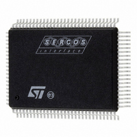
ST92F150JDV1QC STMicroelectronics, ST92F150JDV1QC Datasheet - Page 54

ST92F150JDV1QC
Manufacturer Part Number
ST92F150JDV1QC
Description
IC MCU 128K FLASH 100-PQFP
Manufacturer
STMicroelectronics
Series
ST9r
Datasheet
1.ST92F150CV1TB.pdf
(429 pages)
Specifications of ST92F150JDV1QC
Core Processor
ST9
Core Size
8/16-Bit
Speed
24MHz
Connectivity
CAN, I²C, LIN, SCI, SPI
Peripherals
DMA, LVD, POR, PWM, WDT
Number Of I /o
77
Program Memory Size
128KB (128K x 8)
Program Memory Type
FLASH
Eeprom Size
1K x 8
Ram Size
6K x 8
Voltage - Supply (vcc/vdd)
4.5 V ~ 5.5 V
Data Converters
A/D 16x10b
Oscillator Type
Internal
Operating Temperature
-40°C ~ 125°C
Package / Case
100-QFP
Processor Series
ST92F15x
Core
ST9
Data Bus Width
8 bit, 16 bit
Data Ram Size
6 KB
Interface Type
CAN, I2C, SCI, SPI
Maximum Clock Frequency
24 MHz
Number Of Programmable I/os
80
Number Of Timers
5 x 16 bit
Operating Supply Voltage
4.5 V to 5.5 V
Maximum Operating Temperature
+ 105 C
Mounting Style
SMD/SMT
Development Tools By Supplier
ST92F150-EPB
Minimum Operating Temperature
- 40 C
On-chip Adc
16 bit x 10 bit
Case
QFP
Lead Free Status / RoHS Status
Lead free / RoHS Compliant
Other names
497-2137
Available stocks
Company
Part Number
Manufacturer
Quantity
Price
- Current page: 54 of 429
- Download datasheet (8Mb)
ST92F124/F150/F250 - SINGLE VOLTAGE FLASH & E3 TM (EMULATED EEPROM)
FUNCTIONAL DESCRIPTION (Cont’d)
3.2.3 Operation
The memory has a register interface mapped in
memory space (segment 22h). All operations are
enabled through the FCR (Flash Control Register),
ECR (
All operations on the Flash must be executed from
another memory (internal RAM,
memory).
Flash (including TestFlash) and
pendent, this means that one can be read while
the other is written. However simultaneous Flash
and
An interrupt can be generated at the end of a
Flash or an
multiplexed with an external interrupt EXTINTx
(device dependent) to generate an interrupt INTx.
The status of a write operation inside the Flash
and the
the FESR[1:0] registers.
Control and Status registers are mapped in mem-
ory (segment 22h), as shown in the following fig-
ure.
Figure 32. Control and Status Register Map.
In order to use the same data pointer register
(DPR) to point both to the
2203FFh) and to these control and status regis-
ters, the Flash and
mapped not only at page 0x89 (224000h-
224003h) but also on page 0x88 (221000h-
221003h).
54/429
9
224000h
224001h
224002h
224003h
E
3 TM
E
3 TM
E
3 TM
write operations are forbidden.
/
/
/
Control Register).
/
E
221000h
221001h
221002h
221003h
memories can be monitored through
3 TM
write operation: this interrupt is
Register Interface
E
3 TM
control registers are
FESR0
FESR1
FCR
ECR
E
3 TM
E
E
3 TM
3 TM
(220000h-
, external
are inde-
If the RESET pin is activated during a write opera-
tion, the write operation is interrupted. In this case
the user must repeat this last write operation fol-
lowing power on or reset. If the internal supply volt-
age drops below the V
quence is generated automatically by hardware.
3.2.4
The update of the
pages of 16 consecutive bytes. The Page Update
operation allows up to 16 bytes to be loaded into
the RAM buffer that replace the ones already con-
tained in the specified address.
Each time a Page Update operation is executed in
the
in the next free block relative to the specified page
(the RAM buffer is previously automatically filled
with old data for all the page addresses not select-
ed for updating). If all the 4 blocks of the specified
page in the current
content is copied to the complementary sector,
that becomes the new current one.
After that the specified page has been copied to
the next free block, one erase phase is executed
on the complementary sector, if the 4 erase phas-
es have not yet been executed. When the selected
page is copied to the complementary sector, the
remaining 63 pages are also copied to the first
block of the new sector; then the first erase phase
is executed on the previous full sector. All this is
executed in a hidden manner, and the End Page
Update Interrupt is generated only after the end of
the complete operation.
At Reset the two status pages are read in order to
detect which is the sector that is currently mapping
the
mapped. A system defined routine written in Test-
Flash is executed at reset, so that any previously
aborted write operation is restarted and complet-
ed.
E
E
3 TM
E
3 TM
3 TM
, the RAM buffer content is programmed
, and in which block each page is
Update Operation
E
E
3 TM
3 TM
IT-
content can be made by
sector are full, the page
threshold, a reset se-
Related parts for ST92F150JDV1QC
Image
Part Number
Description
Manufacturer
Datasheet
Request
R

Part Number:
Description:
BOARD PROGRAM FOR ST92F150 MCU
Manufacturer:
STMicroelectronics
Datasheet:

Part Number:
Description:
BOARD EVALUATION FOR ST9 SERIES
Manufacturer:
STMicroelectronics
Datasheet:

Part Number:
Description:
BOARD EMULATOR FOR ST9 SERIES
Manufacturer:
STMicroelectronics
Datasheet:

Part Number:
Description:
MCU, MPU & DSP Development Tools ST9 Dedication Board
Manufacturer:
STMicroelectronics
Datasheet:

Part Number:
Description:
STMicroelectronics [RIPPLE-CARRY BINARY COUNTER/DIVIDERS]
Manufacturer:
STMicroelectronics
Datasheet:

Part Number:
Description:
STMicroelectronics [LIQUID-CRYSTAL DISPLAY DRIVERS]
Manufacturer:
STMicroelectronics
Datasheet:

Part Number:
Description:
BOARD EVAL FOR MEMS SENSORS
Manufacturer:
STMicroelectronics
Datasheet:

Part Number:
Description:
NPN TRANSISTOR POWER MODULE
Manufacturer:
STMicroelectronics
Datasheet:

Part Number:
Description:
TURBOSWITCH ULTRA-FAST HIGH VOLTAGE DIODE
Manufacturer:
STMicroelectronics
Datasheet:

Part Number:
Description:
Manufacturer:
STMicroelectronics
Datasheet:

Part Number:
Description:
DIODE / SCR MODULE
Manufacturer:
STMicroelectronics
Datasheet:

Part Number:
Description:
DIODE / SCR MODULE
Manufacturer:
STMicroelectronics
Datasheet:


