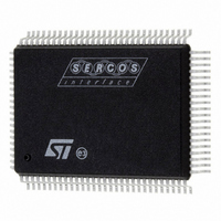
ST92F150JDV1QC STMicroelectronics, ST92F150JDV1QC Datasheet - Page 264

ST92F150JDV1QC
Manufacturer Part Number
ST92F150JDV1QC
Description
IC MCU 128K FLASH 100-PQFP
Manufacturer
STMicroelectronics
Series
ST9r
Datasheet
1.ST92F150CV1TB.pdf
(429 pages)
Specifications of ST92F150JDV1QC
Core Processor
ST9
Core Size
8/16-Bit
Speed
24MHz
Connectivity
CAN, I²C, LIN, SCI, SPI
Peripherals
DMA, LVD, POR, PWM, WDT
Number Of I /o
77
Program Memory Size
128KB (128K x 8)
Program Memory Type
FLASH
Eeprom Size
1K x 8
Ram Size
6K x 8
Voltage - Supply (vcc/vdd)
4.5 V ~ 5.5 V
Data Converters
A/D 16x10b
Oscillator Type
Internal
Operating Temperature
-40°C ~ 125°C
Package / Case
100-QFP
Processor Series
ST92F15x
Core
ST9
Data Bus Width
8 bit, 16 bit
Data Ram Size
6 KB
Interface Type
CAN, I2C, SCI, SPI
Maximum Clock Frequency
24 MHz
Number Of Programmable I/os
80
Number Of Timers
5 x 16 bit
Operating Supply Voltage
4.5 V to 5.5 V
Maximum Operating Temperature
+ 105 C
Mounting Style
SMD/SMT
Development Tools By Supplier
ST92F150-EPB
Minimum Operating Temperature
- 40 C
On-chip Adc
16 bit x 10 bit
Case
QFP
Lead Free Status / RoHS Status
Lead free / RoHS Compliant
Other names
497-2137
Available stocks
Company
Part Number
Manufacturer
Quantity
Price
- Current page: 264 of 429
- Download datasheet (8Mb)
I2C BUS INTERFACE
I
The following seven registers are used to handle
the interrupt and the DMA features:
– Interrupt Status Register I2CISR
– Interrupt Mask Register I2CIMR
– Interrupt Vector Register I2CIVR
– Receiver DMA Address Pointer Register
– Receiver DMA Transaction Counter Register
– Transmitter DMA Address Pointer Register
– Transmitter DMA transaction Counter Register
The interface can decode both addresses:
– Software programmable 7-bit General Call
– I
After a reset, the interface is disabled.
IMPORTANT:
1. To guarantee correct operation, before enabling
the peripheral (while I2CCR.PE=0), configure bit7
and bit6 of the I2COAR2 register according to the
internal clock INTCLK (for example 11xxxxxxb in
the range 14 - 30 MHz).
2. Bit7 of the I2CCR register must be cleared.
10.8.3.1 Mode Selection
In I
following modes:
– Master transmitter/receiver
– Slave transmitter/receiver
By default, it operates in slave mode.
This interface automatically switches from slave to
master after a start condition is generated on the
bus and from master to slave in case of arbitration
loss or stop condition generation.
In Master mode, it initiates a data transfer and
generates the clock signal. A serial data transfer
always begins with a start condition and ends with
a stop condition. Both start and stop conditions are
generated in master mode by software.
In Slave mode, it is able to recognize its own ad-
dress (7 or 10-bit), as stored in the I2COAR1 and
I2COAR2 registers and (when the I2CCR.ENGC
264/429
9
2
C BUS INTERFACE (Cont’d)
I2CRDAP
I2CRDC
I2CTDAP
I2CTDC
address
register in 7-bit address mode or stored in
I2COAR1 and I2COAR2 registers in 10-bit ad-
dress mode.
2
2
C address stored by software in the I2COAR1
C mode, the interface can operate in the four
bit is set) the General Call address (stored in
I2CADR register). It never recognizes the Start
Byte (address byte 01h) whatever its own address
is.
Data and addresses are transferred in 8 bits, MSB
first. The first byte(s) following the start condition
contain the address (one byte in 7-bit mode, two
bytes in 10-bit mode). The address is always
transmitted in master mode.
A 9th clock pulse follows the 8 clock cycles of a
byte transfer, during which the receiver must send
an
Acknowledge is enabled and disabled by software.
Refer to
acknowledge
Figure
127.
bit
to
the
transmitter.
Related parts for ST92F150JDV1QC
Image
Part Number
Description
Manufacturer
Datasheet
Request
R

Part Number:
Description:
BOARD PROGRAM FOR ST92F150 MCU
Manufacturer:
STMicroelectronics
Datasheet:

Part Number:
Description:
BOARD EVALUATION FOR ST9 SERIES
Manufacturer:
STMicroelectronics
Datasheet:

Part Number:
Description:
BOARD EMULATOR FOR ST9 SERIES
Manufacturer:
STMicroelectronics
Datasheet:

Part Number:
Description:
MCU, MPU & DSP Development Tools ST9 Dedication Board
Manufacturer:
STMicroelectronics
Datasheet:

Part Number:
Description:
STMicroelectronics [RIPPLE-CARRY BINARY COUNTER/DIVIDERS]
Manufacturer:
STMicroelectronics
Datasheet:

Part Number:
Description:
STMicroelectronics [LIQUID-CRYSTAL DISPLAY DRIVERS]
Manufacturer:
STMicroelectronics
Datasheet:

Part Number:
Description:
BOARD EVAL FOR MEMS SENSORS
Manufacturer:
STMicroelectronics
Datasheet:

Part Number:
Description:
NPN TRANSISTOR POWER MODULE
Manufacturer:
STMicroelectronics
Datasheet:

Part Number:
Description:
TURBOSWITCH ULTRA-FAST HIGH VOLTAGE DIODE
Manufacturer:
STMicroelectronics
Datasheet:

Part Number:
Description:
Manufacturer:
STMicroelectronics
Datasheet:

Part Number:
Description:
DIODE / SCR MODULE
Manufacturer:
STMicroelectronics
Datasheet:

Part Number:
Description:
DIODE / SCR MODULE
Manufacturer:
STMicroelectronics
Datasheet:


