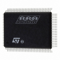
ST92F150JDV1QC STMicroelectronics, ST92F150JDV1QC Datasheet - Page 68

ST92F150JDV1QC
Manufacturer Part Number
ST92F150JDV1QC
Description
IC MCU 128K FLASH 100-PQFP
Manufacturer
STMicroelectronics
Series
ST9r
Datasheet
1.ST92F150CV1TB.pdf
(429 pages)
Specifications of ST92F150JDV1QC
Core Processor
ST9
Core Size
8/16-Bit
Speed
24MHz
Connectivity
CAN, I²C, LIN, SCI, SPI
Peripherals
DMA, LVD, POR, PWM, WDT
Number Of I /o
77
Program Memory Size
128KB (128K x 8)
Program Memory Type
FLASH
Eeprom Size
1K x 8
Ram Size
6K x 8
Voltage - Supply (vcc/vdd)
4.5 V ~ 5.5 V
Data Converters
A/D 16x10b
Oscillator Type
Internal
Operating Temperature
-40°C ~ 125°C
Package / Case
100-QFP
Processor Series
ST92F15x
Core
ST9
Data Bus Width
8 bit, 16 bit
Data Ram Size
6 KB
Interface Type
CAN, I2C, SCI, SPI
Maximum Clock Frequency
24 MHz
Number Of Programmable I/os
80
Number Of Timers
5 x 16 bit
Operating Supply Voltage
4.5 V to 5.5 V
Maximum Operating Temperature
+ 105 C
Mounting Style
SMD/SMT
Development Tools By Supplier
ST92F150-EPB
Minimum Operating Temperature
- 40 C
On-chip Adc
16 bit x 10 bit
Case
QFP
Lead Free Status / RoHS Status
Lead free / RoHS Compliant
Other names
497-2137
Available stocks
Company
Part Number
Manufacturer
Quantity
Price
- Current page: 68 of 429
- Download datasheet (8Mb)
ST92F124/F150/F250 - REGISTER AND MEMORY MAP
4 REGISTER AND MEMORY MAP
4.1 INTRODUCTION
The ST92F124/F150/F250 register map, memory
map and peripheral options are documented in
this section. Use this reference information to sup-
plement the functional descriptions given else-
where in this document.
4.2 MEMORY CONFIGURATION
The Program memory space of the ST92F124/
F150/F250 up to 256K bytes of directly addressa-
ble on-chip memory, is fully available to the user.
4.2.1 Reset Vector Location
The user power on reset vector must be stored in
the first two physical bytes of memory, 000000h
and 000001h.
4.2.2 Location of Vector for External Watchdog
Refresh
If an external watchdog is used, it must be re-
freshed during TestFlash execution by a user writ-
ten routine. This routine has to be located in Flash
memory, the address where the routine starts has
to be written in 000006h (one word) while the seg-
68/429
9
ment where the routine is located has to be written
in 000009h (one byte).
This routine is called at least once every time that
the TestFlash executes an E
the write operation has a long duration, the user
routine is called with a rate fixed by location
000008h with an internal clock frequency of 2
MHz, location 000008h fixes the number of milli-
seconds to wait between two calls of the user rou-
tine.
Table 14. User Routine Parameters
If location 000006h to 000007h is virgin (FFFFh),
the user routine is not called.
Location
000006h to
000007h
000008h
000009h
Size
2 bytes
1 byte
1 byte
Description
User routine address
ms rate at 2 MHz.
User routine segment
3 TM
write operation. If
Related parts for ST92F150JDV1QC
Image
Part Number
Description
Manufacturer
Datasheet
Request
R

Part Number:
Description:
BOARD PROGRAM FOR ST92F150 MCU
Manufacturer:
STMicroelectronics
Datasheet:

Part Number:
Description:
BOARD EVALUATION FOR ST9 SERIES
Manufacturer:
STMicroelectronics
Datasheet:

Part Number:
Description:
BOARD EMULATOR FOR ST9 SERIES
Manufacturer:
STMicroelectronics
Datasheet:

Part Number:
Description:
MCU, MPU & DSP Development Tools ST9 Dedication Board
Manufacturer:
STMicroelectronics
Datasheet:

Part Number:
Description:
STMicroelectronics [RIPPLE-CARRY BINARY COUNTER/DIVIDERS]
Manufacturer:
STMicroelectronics
Datasheet:

Part Number:
Description:
STMicroelectronics [LIQUID-CRYSTAL DISPLAY DRIVERS]
Manufacturer:
STMicroelectronics
Datasheet:

Part Number:
Description:
BOARD EVAL FOR MEMS SENSORS
Manufacturer:
STMicroelectronics
Datasheet:

Part Number:
Description:
NPN TRANSISTOR POWER MODULE
Manufacturer:
STMicroelectronics
Datasheet:

Part Number:
Description:
TURBOSWITCH ULTRA-FAST HIGH VOLTAGE DIODE
Manufacturer:
STMicroelectronics
Datasheet:

Part Number:
Description:
Manufacturer:
STMicroelectronics
Datasheet:

Part Number:
Description:
DIODE / SCR MODULE
Manufacturer:
STMicroelectronics
Datasheet:

Part Number:
Description:
DIODE / SCR MODULE
Manufacturer:
STMicroelectronics
Datasheet:


