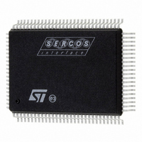
ST92F150JDV1QC STMicroelectronics, ST92F150JDV1QC Datasheet - Page 345

ST92F150JDV1QC
Manufacturer Part Number
ST92F150JDV1QC
Description
IC MCU 128K FLASH 100-PQFP
Manufacturer
STMicroelectronics
Series
ST9r
Datasheet
1.ST92F150CV1TB.pdf
(429 pages)
Specifications of ST92F150JDV1QC
Core Processor
ST9
Core Size
8/16-Bit
Speed
24MHz
Connectivity
CAN, I²C, LIN, SCI, SPI
Peripherals
DMA, LVD, POR, PWM, WDT
Number Of I /o
77
Program Memory Size
128KB (128K x 8)
Program Memory Type
FLASH
Eeprom Size
1K x 8
Ram Size
6K x 8
Voltage - Supply (vcc/vdd)
4.5 V ~ 5.5 V
Data Converters
A/D 16x10b
Oscillator Type
Internal
Operating Temperature
-40°C ~ 125°C
Package / Case
100-QFP
Processor Series
ST92F15x
Core
ST9
Data Bus Width
8 bit, 16 bit
Data Ram Size
6 KB
Interface Type
CAN, I2C, SCI, SPI
Maximum Clock Frequency
24 MHz
Number Of Programmable I/os
80
Number Of Timers
5 x 16 bit
Operating Supply Voltage
4.5 V to 5.5 V
Maximum Operating Temperature
+ 105 C
Mounting Style
SMD/SMT
Development Tools By Supplier
ST92F150-EPB
Minimum Operating Temperature
- 40 C
On-chip Adc
16 bit x 10 bit
Case
QFP
Lead Free Status / RoHS Status
Lead free / RoHS Compliant
Other names
497-2137
Available stocks
Company
Part Number
Manufacturer
Quantity
Price
- Current page: 345 of 429
- Download datasheet (8Mb)
CONTROLLER AREA NETWORK (Cont’d)
Bit 4 = TXOK0 Transmission OK for mailbox 0
- Read
This bit is set by hardware when the transmission
request on mailbox 0 has been completed suc-
cessfully. Please refer to
This bit is cleared by hardware when mailbox 0 is
requested for transmission or when the software
clears the RQCP0 bit.
Bit 3 = Reserved. Forced to 0 by hardware.
Bit 2 = RQCP2 Request Completed for Mailbox 2
- Read/Clear
This bit is set by hardware to signal that the last re-
quest for mailbox 2 has been completed. The re-
quest could be a transmit or an abort request.
This bit is cleared by software.
Bit 1 = RQCP1 Request Completed for Mailbox 1
- Read/Clear
This bit is set by hardware to signal that the last re-
quest for mailbox 1 has been completed. The re-
quest could be a transmit or an abort request.
This bit is cleared by software.
Bit 0 = RQCP0 Request Completed for Mailbox 0
- Read/Clear
This bit is set by hardware to signal that the last re-
quest for mailbox 0 has been completed. The re-
quest could be a transmit or an abort request.
This bit is cleared by software.
CAN TRANSMIT PRIORITY REGISTER (CTPR)
All bits of this register are read only.
Reset Value: 0000 0000 (00h)
Bit 7 = LOW2 Lowest Priority Flag for Mailbox 2
- Read
This bit is set by hardware when more than one
mailbox are pending for transmission and mailbox
2 has the lowest priority.
LOW2
7
LOW1
LOW0
TME2
Figure
TME1
147.
TME0
CODE1 CODE0
0
CONTROLLER AREA NETWORK (bxCAN)
Bit 6 = LOW1 Lowest Priority Flag for Mailbox 1
- Read
This bit is set by hardware when more than one
mailbox are pending for transmission and mailbox
1 has the lowest priority.
Bit 5 = LOW0 Lowest Priority Flag for Mailbox 0
- Read
This bit is set by hardware when more than one
mailbox are pending for transmission and mailbox
0 has the lowest priority.
Note: These bits are set to zero when only one
mailbox is pending.
Bit 4 = TME2 Transmit Mailbox 2 Empty
- Read
This bit is set by hardware when no transmit re-
quest is pending for mailbox 2.
Bit 3 = TME1 Transmit Mailbox 1 Empty
- Read
This bit is set by hardware when no transmit re-
quest is pending for mailbox 1.
Bit 2 = TME0 Transmit Mailbox 0 Empty
- Read
This bit is set by hardware when no transmit re-
quest is pending for mailbox 0.
Bit 1:0 = CODE[1:0] Mailbox Code
- Read
In case at least one transmit mailbox is free, the
code value is equal to the number of the next
transmit mailbox free.
In case all transmit mailboxes are pending, the
code value is equal to the number of the transmit
mailbox with the lowest priority.
345/429
9
Related parts for ST92F150JDV1QC
Image
Part Number
Description
Manufacturer
Datasheet
Request
R

Part Number:
Description:
BOARD PROGRAM FOR ST92F150 MCU
Manufacturer:
STMicroelectronics
Datasheet:

Part Number:
Description:
BOARD EVALUATION FOR ST9 SERIES
Manufacturer:
STMicroelectronics
Datasheet:

Part Number:
Description:
BOARD EMULATOR FOR ST9 SERIES
Manufacturer:
STMicroelectronics
Datasheet:

Part Number:
Description:
MCU, MPU & DSP Development Tools ST9 Dedication Board
Manufacturer:
STMicroelectronics
Datasheet:

Part Number:
Description:
STMicroelectronics [RIPPLE-CARRY BINARY COUNTER/DIVIDERS]
Manufacturer:
STMicroelectronics
Datasheet:

Part Number:
Description:
STMicroelectronics [LIQUID-CRYSTAL DISPLAY DRIVERS]
Manufacturer:
STMicroelectronics
Datasheet:

Part Number:
Description:
BOARD EVAL FOR MEMS SENSORS
Manufacturer:
STMicroelectronics
Datasheet:

Part Number:
Description:
NPN TRANSISTOR POWER MODULE
Manufacturer:
STMicroelectronics
Datasheet:

Part Number:
Description:
TURBOSWITCH ULTRA-FAST HIGH VOLTAGE DIODE
Manufacturer:
STMicroelectronics
Datasheet:

Part Number:
Description:
Manufacturer:
STMicroelectronics
Datasheet:

Part Number:
Description:
DIODE / SCR MODULE
Manufacturer:
STMicroelectronics
Datasheet:

Part Number:
Description:
DIODE / SCR MODULE
Manufacturer:
STMicroelectronics
Datasheet:


