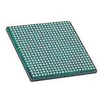
LFXP2-30E-5FN484C LATTICE SEMICONDUCTOR, LFXP2-30E-5FN484C Datasheet - Page 16

LFXP2-30E-5FN484C
Manufacturer Part Number
LFXP2-30E-5FN484C
Description
IC, LATTICEXP2 FPGA, 435MHZ, FPBGA-484
Manufacturer
LATTICE SEMICONDUCTOR
Series
LatticeXP2r
Datasheet
1.LFXP2-5E-5TN144C.pdf
(93 pages)
Specifications of LFXP2-30E-5FN484C
No. Of Logic Blocks
29000
No. Of Macrocells
14500
Family Type
LatticeXP2
No. Of Speed Grades
5
No. Of I/o's
363
Clock Management
PLL
Total Ram Bits
387Kbit
Lead Free Status / RoHS Status
Lead free / RoHS Compliant
Available stocks
Company
Part Number
Manufacturer
Quantity
Price
Company:
Part Number:
LFXP2-30E-5FN484C
Manufacturer:
Lattice Semiconductor Corporation
Quantity:
10 000
Lattice Semiconductor
devices have six secondary clock regions. All devices in the LatticeXP2 family have eight secondary clock
resources per region (SC0 to SC7).
The secondary clock muxes are located in the center of the device. Figure 2-12 shows the mux structure of the
secondary clock routing. Secondary clocks SC0 to SC3 are used for high fan-out control and SC4 to SC7 are used
for clock signals.
Figure 2-11. Secondary Clock Regions XP2-40
Figure 2-12. Per Region Secondary Clock Selection
SC0
4:1
Secondary Clock
Secondary Clock
Secondary Clock
Secondary Clock
I/O Bank 0
I/O Bank 5
Region 1
SC1
Region 2
Region 3
Region 4
4:1
Secondary Clock Feedlines: 8 PIOs + 16 Routing
8 Secondary Clocks (SC0 to SC7) per Region
SC2
4:1
SC3
4:1
Clock/Control
SC4
2-13
Secondary Clock
Secondary Clock
Secondary Clock
Secondary Clock
4:1
Region 5
I/O Bank 1
Region 6
Region 7
Region 8
I/O Bank 4
SC5
4:1
SC6
4:1
LatticeXP2 Family Data Sheet
SC7
4:1
Vertical Routing
Channel Regional
Boundary
EBR Row
Regional
Boundary
EBR Row
Regional
Boundary
DSP Row
Regional
Boundary
Architecture


