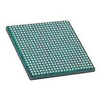
LFXP2-30E-5FN484C LATTICE SEMICONDUCTOR, LFXP2-30E-5FN484C Datasheet - Page 41

LFXP2-30E-5FN484C
Manufacturer Part Number
LFXP2-30E-5FN484C
Description
IC, LATTICEXP2 FPGA, 435MHZ, FPBGA-484
Manufacturer
LATTICE SEMICONDUCTOR
Series
LatticeXP2r
Datasheet
1.LFXP2-5E-5TN144C.pdf
(93 pages)
Specifications of LFXP2-30E-5FN484C
No. Of Logic Blocks
29000
No. Of Macrocells
14500
Family Type
LatticeXP2
No. Of Speed Grades
5
No. Of I/o's
363
Clock Management
PLL
Total Ram Bits
387Kbit
Lead Free Status / RoHS Status
Lead free / RoHS Compliant
Available stocks
Company
Part Number
Manufacturer
Quantity
Price
Company:
Part Number:
LFXP2-30E-5FN484C
Manufacturer:
Lattice Semiconductor Corporation
Quantity:
10 000
Lattice Semiconductor
and loaded directly onto test nodes, or test data to be captured and shifted out for verification. The test access port
consists of dedicated I/Os: TDI, TDO, TCK and TMS. The test access port has its own supply voltage V
operate with LVCMOS3.3, 2.5, 1.8, 1.5 and 1.2 standards. For more information, please see TN1141, LatticeXP2
sysCONFIG Usage Guide.
flexiFLASH Device Configuration
The LatticeXP2 devices combine Flash and SRAM on a single chip to provide users with flexibility in device pro-
gramming and configuration. Figure 2-33 provides an overview of the arrangement of Flash and SRAM configura-
tion cells within the device. The remainder of this section provides an overview of these capabilities. See TN1141,
LatticeXP2 sysCONFIG Usage Guide, for a more detailed description.
Figure 2-33. Overview of Flash and SRAM Configuration Cells Within LatticeXP2 Devices
At power-up, or on user command, data is transferred from the on-chip Flash memory to the SRAM configuration
cells that control the operation of the device. This is done with massively parallel buses enabling the parts to oper-
ate within microseconds of the power supplies reaching valid levels; this capability is referred to as Instant-On.
The on-chip Flash enables a single-chip solution eliminating the need for external boot memory. This Flash can be
programmed through either the JTAG or Slave SPI ports of the device. The SRAM configuration space can also be
infinitely reconfigured through the JTAG and Master SPI ports. The JTAG port is IEEE 1149.1 and IEEE 1532 com-
pliant.
As described in the EBR section of the data sheet, the FlashBAK capability of the parts enables the contents of the
EBR blocks to be written back into the Flash storage area without erasing or reprogramming other aspects of the
device configuration. Serial TAG memory is also available to allow the storage of small amounts of data such as
calibration coefficients and error codes.
For applications where security is important, the lack of an external bitstream provides a solution that is inherently
more secure than SRAM only FPGAs. This is further enhanced by device locking. The device can be in one of three
modes:
Configuration
EBR Blocks
EBR Blocks
Decryption
and Device
SRAM
Lock
Bits
2-38
Memory
TAG
LatticeXP2 Family Data Sheet
SPI and JTAG
Massively Parallel
Data Transfer
Device Lock
Single-Chip
Instant-ON
for Design
FlashBAK
Flash for
Solution
Security
for EBR
Storage
Architecture
CCJ
and can


