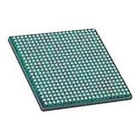
LFXP2-30E-5FN484C LATTICE SEMICONDUCTOR, LFXP2-30E-5FN484C Datasheet - Page 46

LFXP2-30E-5FN484C
Manufacturer Part Number
LFXP2-30E-5FN484C
Description
IC, LATTICEXP2 FPGA, 435MHZ, FPBGA-484
Manufacturer
LATTICE SEMICONDUCTOR
Series
LatticeXP2r
Datasheet
1.LFXP2-5E-5TN144C.pdf
(93 pages)
Specifications of LFXP2-30E-5FN484C
No. Of Logic Blocks
29000
No. Of Macrocells
14500
Family Type
LatticeXP2
No. Of Speed Grades
5
No. Of I/o's
363
Clock Management
PLL
Total Ram Bits
387Kbit
Lead Free Status / RoHS Status
Lead free / RoHS Compliant
Available stocks
Company
Part Number
Manufacturer
Quantity
Price
Company:
Part Number:
LFXP2-30E-5FN484C
Manufacturer:
Lattice Semiconductor Corporation
Quantity:
10 000
Lattice Semiconductor
Hot Socketing Specifications
DC Electrical Characteristics
I
1. Insensitive to sequence of V
2. 0 ≤ V
3. I
4. LVCMOS and LVTTL only.
5. Initial production device. For the first 20ns after hot insertion, current specification is 8mA.
Note: Specifications for the LFXP2-17E ‘8W’ are the same as the LFXP2-17E, except as specified above in the
Hot Socketing Specifications and DC Electrical Characteristics Tables.
I
I
I
I
I
I
I
V
C1
C2
1. Input or I/O leakage current is measured with the pin configured as an input or as an I/O with the output driver tri-stated. It is not measured
2. Specified limits do not apply to the single I/O, PL26B, for the LFXP2-17E-8W.
3. T
DK
Symbol
IL
PU
PD
BHLS
BHHS
BHLO
BHHO
BHT
, I
Symbol
with the output driver active. Bus maintenance circuits are disabled.
DK
A
IH
25
is additive to I
1, 2
CC
o
C, f = 1.0MHz.
≤ V
Input or I/O Low Leakage
I/O Active Pull-up Current
I/O Active Pull-down Current
Bus Hold Low Sustaining Current V
Bus Hold High Sustaining Current V
Bus Hold Low Overdrive Current 0 ≤ V
Bus Hold High Overdrive Current 0 ≤ V
Bus Hold Trip Points
I/O Capacitance
Dedicated Input Capacitance
CC
Input or I/O Leakage Current
LFXP2-17E-8W
Leakage Current
(MAX), 0 ≤ V
PU
, I
Parameter
PW
or I
3
CCIO
Parameter
CC
BH
, V
5
.
I/O PL26B
≤ V
CCAUX
CCIO
Over Recommended Operating Conditions
and V
2
(MAX) or 0 ≤ V
CCIO
0 ≤ V
V
0 ≤ V
V
V
V
V
V
CCIO
IL
IN
IN
CCIO
CC
CCIO
CC
. However, assumes monotonic rise/fall rates for V
1, 2, 3, 4
(MAX) ≤ V
= V
= 0.7 V
= 1.2V, V
= 1.2V, V
IN
IN
IN
IN
≤ V
= 3.3V, 2.5V, 1.8V, 1.5V, 1.2V,
= 3.3V, 2.5V, 1.8V, 1.5V, 1.2V,
IL
≤ V
≤ 0.7 V
≤ V
≤ V
0 ≤ V
0 ≤ V
CCAUX
(MAX)
IN
CCIO
CCIO
CCIO
CCIO
≤ V
IN
IN
IO
IO
≤ V
IN
Condition
CCIO
≤ V
≤ V
IH
= 0 to V
= 0 to V
3-2
≤ V
CCAUX
Condition
(MAX)
IH
IH
CCIO
(MAX.)
(MAX.)
(MAX).
IH
IH
(MAX)
(MAX)
DC and Switching Characteristics
LatticeXP2 Family Data Sheet
V
IL
Min.
—
—
Min.
-30
-30
(MAX)
30
30
—
—
—
—
—
—
CC
, V
CCAUX
Typ.
+/-8
—
Typ.
—
—
—
—
—
—
—
—
—
8
6
and V
V
Max.
CCIO
+/-1
IH
—
Max.
-150
-150
150
210
210
10
—
—
—
—
(MIN)
.
Units
Units
mA
mA
µA
µA
µA
µA
µA
µA
µA
µA
pf
pf
V


