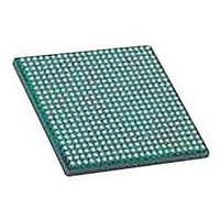
LFXP2-30E-5FN484C LATTICE SEMICONDUCTOR, LFXP2-30E-5FN484C Datasheet - Page 45

LFXP2-30E-5FN484C
Manufacturer Part Number
LFXP2-30E-5FN484C
Description
IC, LATTICEXP2 FPGA, 435MHZ, FPBGA-484
Manufacturer
LATTICE SEMICONDUCTOR
Series
LatticeXP2r
Datasheet
1.LFXP2-5E-5TN144C.pdf
(93 pages)
Specifications of LFXP2-30E-5FN484C
No. Of Logic Blocks
29000
No. Of Macrocells
14500
Family Type
LatticeXP2
No. Of Speed Grades
5
No. Of I/o's
363
Clock Management
PLL
Total Ram Bits
387Kbit
Lead Free Status / RoHS Status
Lead free / RoHS Compliant
Available stocks
Company
Part Number
Manufacturer
Quantity
Price
Company:
Part Number:
LFXP2-30E-5FN484C
Manufacturer:
Lattice Semiconductor Corporation
Quantity:
10 000
April 2008
Absolute Maximum Ratings
Recommended Operating Conditions
On-Chip Flash Memory Specifications
© 2008 Lattice Semiconductor Corp. All Lattice trademarks, registered trademarks, patents, and disclaimers are as listed at www.latticesemi.com/legal. All other brand
or product names are trademarks or registered trademarks of their respective holders. The specifications and information herein are subject to change without notice.
www.latticesemi.com
Supply Voltage V
Supply Voltage V
Supply Voltage V
Supply Voltage V
Output Supply Voltage V
Input or I/O Tristate Voltage Applied
Storage Temperature (Ambient) . . . . . . . . . -65 to 150°C
Junction Temperature Under Bias (Tj) . . . . . . . . . +125°C
1. Stress above those listed under the “Absolute Maximum Ratings” may cause permanent damage to the device. Functional operation of the
2. Compliance with the Lattice Thermal Management document is required.
3. All voltages referenced to GND.
4. V
5. Overshoot and undershoot of -2V to (V
V
V
V
V
V
t
t
1. V
2. If V
3. See recommended voltages by I/O standard in subsequent table.
4. To ensure proper I/O behavior, V
N
t
JCOM
JIND
RETENTION
CC
CCAUX
CCPLL
CCIO
CCJ
PROGCYC
device at these or any other conditions above those indicated in the operational sections of this specification is not implied.
nected to the same power supply as V
CCPLL
CCPLL
2
CCIO
2, 3, 4
1
4
Symbol
Symbol
only available on csBGA, PQFP and TQFP packages.
only available on csBGA, PQFP and TQFP packages.
or V
CCJ
is set to 1.2V, they must be connected to the same power supply as V
CC
CCAUX
CCJ
CCPLL
. . . . . . . . . . . . . . . . . . . -0.5 to 1.32V
. . . . . . . . . . . . . . . . . . -0.5 to 3.75V
Core Supply Voltage
Auxiliary Supply Voltage
PLL Supply Voltage
I/O Driver Supply Voltage
Supply Voltage for IEEE 1149.1 Test Access Port
Junction Temperature, Commercial Operation
Junction Temperature, Industrial Operation
Flash Programming Cycles per t
Flash Functional Programming Cycles
Data Retention
4
. . . . . . . . . . . . . . . . -0.5 to 3.75V
. . . . . . . . . . . . . . . . -0.5 to 3.75V
CCIO
CCIO
. . . . . . . . . . . -0.5 to 3.75V
must be turned off at the same time or earlier than V
CCAUX
IHMAX
5
. . . . . . -0.5 to 3.75V
.
+ 2) volts is permitted for a duration of <20ns.
DC and Switching Characteristics
1, 2, 3
Parameter
LatticeXP2 Family Data Sheet
RETENTION
Parameter
3-1
CC.
If V
CCAUX.
CCIO
or V
Preliminary Data Sheet DS1009
DS1009
CCJ
3.135
3.135
Min.
1.14
1.14
1.14
is set to 3.3V, they must be con-
-40
0
DC and Switching_01.4
100,000
10,000
3.465
3.465
3.465
3.465
Max.
Max.
1.26
100
85
20
Cycles
Units
Units
Years
°C
°C
V
V
V
V
V


