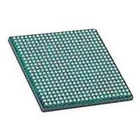
LFXP2-30E-5FN484C LATTICE SEMICONDUCTOR, LFXP2-30E-5FN484C Datasheet - Page 24

LFXP2-30E-5FN484C
Manufacturer Part Number
LFXP2-30E-5FN484C
Description
IC, LATTICEXP2 FPGA, 435MHZ, FPBGA-484
Manufacturer
LATTICE SEMICONDUCTOR
Series
LatticeXP2r
Datasheet
1.LFXP2-5E-5TN144C.pdf
(93 pages)
Specifications of LFXP2-30E-5FN484C
No. Of Logic Blocks
29000
No. Of Macrocells
14500
Family Type
LatticeXP2
No. Of Speed Grades
5
No. Of I/o's
363
Clock Management
PLL
Total Ram Bits
387Kbit
Lead Free Status / RoHS Status
Lead free / RoHS Compliant
Available stocks
Company
Part Number
Manufacturer
Quantity
Price
Company:
Part Number:
LFXP2-30E-5FN484C
Manufacturer:
Lattice Semiconductor Corporation
Quantity:
10 000
Lattice Semiconductor
MAC sysDSP Element
In this case, the two operands, A and B, are multiplied and the result is added with the previous accumulated value.
This accumulated value is available at the output. The user can enable the input and pipeline registers but the out-
put register is always enabled. The output register is used to store the accumulated value. The Accumulators in the
DSP blocks in LatticeXP2 family can be initialized dynamically. A registered overflow signal is also available. The
overflow conditions are provided later in this document. Figure 2-21 shows the MAC sysDSP element.
Figure 2-21. MAC sysDSP
Multiplicand
Multiplier
Signed A
Signed B
Addn
Accumsload
Serial Register B in
n
Input Data
Register B
n
n
SROB
n
Register
Register
Register
Register
Input
Input
Input
Input
m
Input Data
Register A
m
n
SROA
Serial Register A in
m
Register
Register
Register
Register
Pipeline
Pipeline
Pipeline
Pipeline
m
n
2-21
To Accumulator
To Accumulator
To Accumulator
To Accumulator
Multiplier
Register
Pipeline
x
(default)
m+n
Accumulator
CLK (CLK0,CLK1,CLK2,CLK3)
RST(RST0,RST1,RST2,RST3)
CE (CE0,CE1,CE2,CE3)
LatticeXP2 Family Data Sheet
m+n+16
(default)
Preload
(default)
m+n+16
Architecture
Output
Overflow
signal


