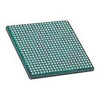
LFXP2-30E-5FN484C LATTICE SEMICONDUCTOR, LFXP2-30E-5FN484C Datasheet - Page 82

LFXP2-30E-5FN484C
Manufacturer Part Number
LFXP2-30E-5FN484C
Description
IC, LATTICEXP2 FPGA, 435MHZ, FPBGA-484
Manufacturer
LATTICE SEMICONDUCTOR
Series
LatticeXP2r
Datasheet
1.LFXP2-5E-5TN144C.pdf
(93 pages)
Specifications of LFXP2-30E-5FN484C
No. Of Logic Blocks
29000
No. Of Macrocells
14500
Family Type
LatticeXP2
No. Of Speed Grades
5
No. Of I/o's
363
Clock Management
PLL
Total Ram Bits
387Kbit
Lead Free Status / RoHS Status
Lead free / RoHS Compliant
Available stocks
Company
Part Number
Manufacturer
Quantity
Price
Company:
Part Number:
LFXP2-30E-5FN484C
Manufacturer:
Lattice Semiconductor Corporation
Quantity:
10 000
Pin Information Summary (Cont.)
Lattice Semiconductor
Logic Signal Connections
Package pinout information can be found under “Data Sheets” on the LatticeXP2 product pages on the Lattice web-
site at www.latticesemi.com/products/fpga/xp2 and in the Lattice ispLEVER software.
Thermal Management
Thermal management is recommended as part of any sound FPGA design methodology. To assess the thermal
characteristics of a system, Lattice specifies a maximum allowable junction temperature in all device data sheets.
Designers must complete a thermal analysis of their specific design to ensure that the device and package do not
exceed the junction temperature limits. Refer to the Thermal Management document to find the device/package
specific thermal values.
For further information regarding Thermal Management, refer to the Thermal Management document located on
the Lattice website at www.latticesemi.com.
For Further Information
• Technical Note TN1139 - Power Estimation and Management for LatticeXP2 Devices
• Power Calculator tool included with Lattice’s ispLEVER design tool, or as a standalone download from
PCI capable I/Os
Bonding Out per
Bank
1. Minimum requirement to implement a fully functional 8-bit wide DDR bus. Available DDR interface consists of at least 12 I/Os (1 DQS + 1 DQSB + 8 DQs + 1
www.latticesemi.com/software
DM + Bank VREF1).
Pin Type
Bank0
Bank1
Bank2
Bank3
Bank4
Bank5
Bank6
Bank7
csBGA
132
18
14
4
0
0
8
0
0
TQFP
144
20
18
6
0
0
8
0
0
XP2-5
PQFP
208
20
18
18
20
0
0
0
0
ftBGA
256
26
18
18
24
0
0
0
0
csBGA
132
18
14
4
0
0
8
0
0
TQFP
144
20
18
6
0
0
8
0
0
XP2-8
4-5
PQFP
208
20
18
18
20
0
0
0
0
ftBGA
256
28
22
26
24
0
0
0
0
PQFP
208
20
18
18
20
0
0
0
0
XP2-17
ftBGA
256
28
22
26
24
0
0
0
0
LatticeXP2 Family Data Sheet
fpBGA
484
52
36
36
52
0
0
0
0
ftBGA
256
28
22
26
24
0
0
0
0
Pinout Information
XP2-30
fpBGA
484
52
36
38
53
0
0
0
0
fpBGA
672
70
54
54
70
0
0
0
0
fpBGA
484
52
36
38
53
0
0
0
0
XP2-40
fpBGA
672
70
70
70
70
0
0
0
0


