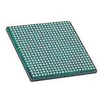
LFXP2-30E-5FN484C LATTICE SEMICONDUCTOR, LFXP2-30E-5FN484C Datasheet - Page 77

LFXP2-30E-5FN484C
Manufacturer Part Number
LFXP2-30E-5FN484C
Description
IC, LATTICEXP2 FPGA, 435MHZ, FPBGA-484
Manufacturer
LATTICE SEMICONDUCTOR
Series
LatticeXP2r
Datasheet
1.LFXP2-5E-5TN144C.pdf
(93 pages)
Specifications of LFXP2-30E-5FN484C
No. Of Logic Blocks
29000
No. Of Macrocells
14500
Family Type
LatticeXP2
No. Of Speed Grades
5
No. Of I/o's
363
Clock Management
PLL
Total Ram Bits
387Kbit
Lead Free Status / RoHS Status
Lead free / RoHS Compliant
Available stocks
Company
Part Number
Manufacturer
Quantity
Price
Company:
Part Number:
LFXP2-30E-5FN484C
Manufacturer:
Lattice Semiconductor Corporation
Quantity:
10 000
Lattice Semiconductor
Switching Test Conditions
Figure 3-12 shows the output test load that is used for AC testing. The specific values for resistance, capacitance,
voltage, and other test conditions are shown in Table 3-6.
Figure 3-12. Output Test Load, LVTTL and LVCMOS Standards
Table 3-6. Test Fixture Required Components, Non-Terminated Interfaces
LVTTL and other LVCMOS settings (L -> H, H -> L)
LVCMOS 2.5 I/O (Z -> H)
LVCMOS 2.5 I/O (Z -> L)
LVCMOS 2.5 I/O (H -> Z)
LVCMOS 2.5 I/O (L -> Z)
Note: Output test conditions for all other interfaces are determined by the respective standards.
Test Condition
*CL Includes Test Fixture and Probe Capacitance
DUT
V
R1
R2
T
1MΩ
100
R
∞
∞
∞
1
3-33
1MΩ
100
R
∞
∞
∞
CL*
2
Test Poi nt
0pF
C
DC and Switching Characteristics
L
LatticeXP2 Family Data Sheet
LVCMOS 3.3 = 1.5V
LVCMOS 2.5 = V
LVCMOS 1.8 = V
LVCMOS 1.5 = V
LVCMOS 1.2 = V
V
V
V
V
OH
OL
CCIO
CCIO
+ 0.10
- 0.10
/2
/2
Timing Ref.
CCIO
CCIO
CCIO
CCIO
/2
/2
/2
/2
V
V
CCIO
CCIO
V
—
—
—
—
—
—
—
T


