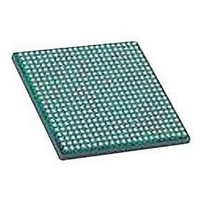
LFXP2-30E-5FN484C LATTICE SEMICONDUCTOR, LFXP2-30E-5FN484C Datasheet - Page 21

LFXP2-30E-5FN484C
Manufacturer Part Number
LFXP2-30E-5FN484C
Description
IC, LATTICEXP2 FPGA, 435MHZ, FPBGA-484
Manufacturer
LATTICE SEMICONDUCTOR
Series
LatticeXP2r
Datasheet
1.LFXP2-5E-5TN144C.pdf
(93 pages)
Specifications of LFXP2-30E-5FN484C
No. Of Logic Blocks
29000
No. Of Macrocells
14500
Family Type
LatticeXP2
No. Of Speed Grades
5
No. Of I/o's
363
Clock Management
PLL
Total Ram Bits
387Kbit
Lead Free Status / RoHS Status
Lead free / RoHS Compliant
Available stocks
Company
Part Number
Manufacturer
Quantity
Price
Company:
Part Number:
LFXP2-30E-5FN484C
Manufacturer:
Lattice Semiconductor Corporation
Quantity:
10 000
Architecture
Lattice Semiconductor
LatticeXP2 Family Data Sheet
If all clock enables remain enabled, the EBR asynchronous reset or GSR may only be applied and released after
the EBR read and write clock inputs are in a steady state condition for a minimum of 1/f
(EBR clock). The reset
MAX
release must adhere to the EBR synchronous reset setup time before the next active read or write clock edge.
If an EBR is pre-loaded during configuration, the GSR input must be disabled or the release of the GSR during
device Wake Up must occur before the release of the device I/Os becoming active.
These instructions apply to all EBR RAM and ROM implementations.
Note that there are no reset restrictions if the EBR synchronous reset is used and the EBR GSR input is disabled.
sysDSP™ Block
The LatticeXP2 family provides a sysDSP block making it ideally suited for low cost, high performance Digital Sig-
nal Processing (DSP) applications. Typical functions used in these applications include Bit Correlators, Fast Fourier
Transform (FFT) functions, Finite Impulse Response (FIR) Filter, Reed-Solomon Encoder/Decoder, Turbo Encoder/
Decoder and Convolutional Encoder/Decoder. These complex signal processing functions use similar building
blocks such as multiply-adders and multiply-accumulators.
sysDSP Block Approach Compare to General DSP
Conventional general-purpose DSP chips typically contain one to four (Multiply and Accumulate) MAC units with
fixed data-width multipliers; this leads to limited parallelism and limited throughput. Their throughput is increased by
higher clock speeds. The LatticeXP2 family, on the other hand, has many DSP blocks that support different data-
widths. This allows the designer to use highly parallel implementations of DSP functions. The designer can opti-
mize the DSP performance vs. area by choosing appropriate levels of parallelism. Figure 2-19 compares the fully
serial and the mixed parallel and serial implementations.
Figure 2-19. Comparison of General DSP and LatticeXP2 Approaches
Operand
Operand
Operand
A
A
A
Operand
Operand
Operand
B
B
B
Operand
Operand
A
B
x
x
x
m/k
Multiplier 0
loops
Multiplier 1
x
M loops
Single
Multiplier k
Multiplier
Accumulator
+ +
(k adds)
Function implemented in
General purpose DSP
m/k
accumulate
Output
Function implemented
in LatticeXP2
sysDSP Block Capabilities
The sysDSP block in the LatticeXP2 family supports four functional elements in three 9, 18 and 36 data path
widths. The user selects a function element for a DSP block and then selects the width and type (signed/unsigned)
of its operands. The operands in the LatticeXP2 family sysDSP Blocks can be either signed or unsigned but not
2-18


