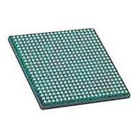
LFXP2-30E-5FN484C LATTICE SEMICONDUCTOR, LFXP2-30E-5FN484C Datasheet - Page 37

LFXP2-30E-5FN484C
Manufacturer Part Number
LFXP2-30E-5FN484C
Description
IC, LATTICEXP2 FPGA, 435MHZ, FPBGA-484
Manufacturer
LATTICE SEMICONDUCTOR
Series
LatticeXP2r
Datasheet
1.LFXP2-5E-5TN144C.pdf
(93 pages)
Specifications of LFXP2-30E-5FN484C
No. Of Logic Blocks
29000
No. Of Macrocells
14500
Family Type
LatticeXP2
No. Of Speed Grades
5
No. Of I/o's
363
Clock Management
PLL
Total Ram Bits
387Kbit
Lead Free Status / RoHS Status
Lead free / RoHS Compliant
Available stocks
Company
Part Number
Manufacturer
Quantity
Price
Company:
Part Number:
LFXP2-30E-5FN484C
Manufacturer:
Lattice Semiconductor Corporation
Quantity:
10 000
Lattice Semiconductor
DQSXFER
LatticeXP2 devices provide a DQSXFER signal to the output buffer to assist it in data transfer to DDR memories
that require DQS strobe be shifted 90
DQSXFER signal runs the span of the data bus.
sysIO Buffer
Each I/O is associated with a flexible buffer referred to as a sysIO buffer. These buffers are arranged around the
periphery of the device in groups referred to as banks. The sysIO buffers allow users to implement the wide variety
of standards that are found in today’s systems including LVCMOS, SSTL, HSTL, LVDS and LVPECL.
sysIO Buffer Banks
LatticeXP2 devices have eight sysIO buffer banks for user I/Os arranged two per side. Each bank is capable of sup-
porting multiple I/O standards. Each sysIO bank has its own I/O supply voltage (V
voltage references, V
shows the eight banks and their associated supplies.
In LatticeXP2 devices, single-ended output buffers and ratioed input buffers (LVTTL, LVCMOS and PCI) are pow-
ered using V
pendent of V
Each bank can support up to two separate V
enced input buffers. Some dedicated I/O pins in a bank can be configured to be a reference voltage supply pin.
Each I/O is individually configurable based on the bank’s supply and reference voltages.
Figure 2-32. LatticeXP2 Banks
CCIO
CCIO
. LVTTL, LVCMOS33, LVCMOS25 and LVCMOS12 can also be set as fixed threshold inputs inde-
.
REF1
V
V REF1(7)
V REF2(7)
V CCIO6
V REF1(6)
V REF2(6)
CCIO7
GND
GND
and V
REF2
, that allow it to be completely independent from the others. Figure 2-32
o
. This shifted DQS strobe is generated by the DQSDEL block. The
REF
Bank 0
Bank 5
voltages, V
BOTTOM
2-34
TOP
REF1
Bank 1
Bank 4
and V
REF2
LatticeXP2 Family Data Sheet
, that set the threshold for the refer-
CCIO
V CCIO2
V REF1(2)
V REF2(2)
V CCIO3
V REF1(3)
V REF2(3)
GND
GND
). In addition, each bank has
Architecture


