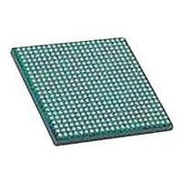
LFXP2-30E-5FN484C LATTICE SEMICONDUCTOR, LFXP2-30E-5FN484C Datasheet - Page 18

LFXP2-30E-5FN484C
Manufacturer Part Number
LFXP2-30E-5FN484C
Description
IC, LATTICEXP2 FPGA, 435MHZ, FPBGA-484
Manufacturer
LATTICE SEMICONDUCTOR
Series
LatticeXP2r
Datasheet
1.LFXP2-5E-5TN144C.pdf
(93 pages)
Specifications of LFXP2-30E-5FN484C
No. Of Logic Blocks
29000
No. Of Macrocells
14500
Family Type
LatticeXP2
No. Of Speed Grades
5
No. Of I/o's
363
Clock Management
PLL
Total Ram Bits
387Kbit
Lead Free Status / RoHS Status
Lead free / RoHS Compliant
Available stocks
Company
Part Number
Manufacturer
Quantity
Price
Company:
Part Number:
LFXP2-30E-5FN484C
Manufacturer:
Lattice Semiconductor Corporation
Quantity:
10 000
Lattice Semiconductor
Figure 2-15. Edge Clock Mux Connections
sysMEM Memory
LatticeXP2 devices contains a number of sysMEM Embedded Block RAM (EBR). The EBR consists of 18 Kbit
RAM with dedicated input and output registers.
sysMEM Memory Block
The sysMEM block can implement single port, dual port or pseudo dual port memories. Each block can be used in
a variety of depths and widths as shown in Table 2-5. FIFOs can be implemented in sysMEM EBR blocks by using
support logic with PFUs. The EBR block supports an optional parity bit for each data byte to facilitate parity check-
ing. EBR blocks provide byte-enable support for configurations with18-bit and 36-bit data widths.
GPLL Output CLKOP
GPLL Output CLKOS
Clock Input Pad
GPLL Input Pad
GPLL Input Pad
Input Pad
Input Pad
Routing
Routing
Routing
2-15
Top and Bottom
ECLK1/ ECLK2
Left and Right
Left and Right
(Both Muxes)
Edge Clocks
Edge Clocks
Edge Clocks
ECLK1
ECLK2
LatticeXP2 Family Data Sheet
Architecture


