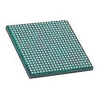
LFXP2-30E-5FN484C LATTICE SEMICONDUCTOR, LFXP2-30E-5FN484C Datasheet - Page 2

LFXP2-30E-5FN484C
Manufacturer Part Number
LFXP2-30E-5FN484C
Description
IC, LATTICEXP2 FPGA, 435MHZ, FPBGA-484
Manufacturer
LATTICE SEMICONDUCTOR
Series
LatticeXP2r
Datasheet
1.LFXP2-5E-5TN144C.pdf
(93 pages)
Specifications of LFXP2-30E-5FN484C
No. Of Logic Blocks
29000
No. Of Macrocells
14500
Family Type
LatticeXP2
No. Of Speed Grades
5
No. Of I/o's
363
Clock Management
PLL
Total Ram Bits
387Kbit
Lead Free Status / RoHS Status
Lead free / RoHS Compliant
Available stocks
Company
Part Number
Manufacturer
Quantity
Price
Company:
Part Number:
LFXP2-30E-5FN484C
Manufacturer:
Lattice Semiconductor Corporation
Quantity:
10 000
February 2008
Features
■ flexiFLASH™ Architecture
■ Live Update Technology
■ sysDSP™ Block
■ Embedded and Distributed Memory
■ sysCLOCK™ PLLs
© 2008 Lattice Semiconductor Corp. All Lattice trademarks, registered trademarks, patents, and disclaimers are as listed at www.latticesemi.com/legal. All other brand
or product names are trademarks or registered trademarks of their respective holders. The specifications and information herein are subject to change without notice.
www.latticesemi.com
Table 1-1. LatticeXP2 Family Selection Guide
Device
LUTs (K)
Distributed RAM (KBits)
EBR SRAM (KBits)
EBR SRAM Blocks
sysDSP Blocks
18 x 18 Multipliers
V
GPLL
Max Available I/O
Packages and I/O Combinations
132-Ball csBGA (8 x 8 mm)
144-Pin TQFP (20 x 20 mm)
208-Pin PQFP (28 x 28 mm)
256-Ball ftBGA (17 x17 mm)
484-Ball fpBGA (23 x 23 mm)
672-Ball fpBGA (27 x 27 mm)
CC
Voltage
• Instant-on
• Infinitely reconfigurable
• Single chip
• FlashBAK™ technology
• Serial TAG memory
• Design security
• TransFR™ technology
• Secure updates with 128 bit AES encryption
• Dual-boot with external SPI
• Three to eight blocks for high performance
• 12 to 32 18x18 multipliers
• Each block supports one 36x36 multiplier or four
• Up to 885 Kbits sysMEM™ EBR
• Up to 83 Kbits Distributed RAM
• Up to four analog PLLs per device
• Clock multiply, divide and phase shifting
Multiply and Accumulate
18x18 or eight 9x9 multipliers
XP2-5
166
172
100
146
1.2
172
10
12
86
5
9
3
2
LatticeXP2 Family Data Sheet
XP2-8
221
201
100
146
201
1.2
18
12
16
86
1-1
8
4
2
■ Flexible I/O Buffer
■ Pre-engineered Source Synchronous
■ Density And Package Options
■ Flexible Device Configuration
■ System Level Support
Interfaces
• sysIO™ buffer supports:
• DDR / DDR2 interfaces up to 200 MHz
• 7:1 LVDS interfaces support display applications
• XGMII
• 5k to 40k LUT4s, 86 to 540 I/Os
• csBGA, TQFP , PQFP , ftBGA and fpBGA packages
• Density migration supported
• SPI (master and slave) Boot Flash Interface
• Dual Boot Image supported
• Soft Error Detect (SED) macro embedded
• IEEE 1149.1 and IEEE 1532 Compliant
• On-chip oscillator for initialization & general use
• Devices operate with 1.2V power supply
– LVCMOS 33/25/18/15/12; LVTTL
– SSTL 33/25/18 class I, II
– HSTL15 class I; HSTL18 class I, II
– PCI
– LVDS, Bus-LVDS, MLVDS, LVPECL, RSDS
XP2-17
276
358
146
201
358
1.2
17
35
15
20
5
4
Preliminary Data Sheet DS1009
XP2-30
Introduction
387
472
201
363
472
1.2
29
56
21
28
7
4
DS1009
Introduction_01.2
XP2-40
885
540
363
540
1.2
40
83
48
32
8
4


