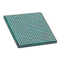
LFXP2-30E-5FN484C LATTICE SEMICONDUCTOR, LFXP2-30E-5FN484C Datasheet - Page 17

LFXP2-30E-5FN484C
Manufacturer Part Number
LFXP2-30E-5FN484C
Description
IC, LATTICEXP2 FPGA, 435MHZ, FPBGA-484
Manufacturer
LATTICE SEMICONDUCTOR
Series
LatticeXP2r
Datasheet
1.LFXP2-5E-5TN144C.pdf
(93 pages)
Specifications of LFXP2-30E-5FN484C
No. Of Logic Blocks
29000
No. Of Macrocells
14500
Family Type
LatticeXP2
No. Of Speed Grades
5
No. Of I/o's
363
Clock Management
PLL
Total Ram Bits
387Kbit
Lead Free Status / RoHS Status
Lead free / RoHS Compliant
Available stocks
Company
Part Number
Manufacturer
Quantity
Price
Company:
Part Number:
LFXP2-30E-5FN484C
Manufacturer:
Lattice Semiconductor Corporation
Quantity:
10 000
Lattice Semiconductor
Slice Clock Selection
Figure 2-13 shows the clock selections and Figure 2-14 shows the control selections for Slice0 through Slice2. All
the primary clocks and the four secondary clocks are routed to this clock selection mux. Other signals, via routing,
can be used as clock inputs to the slices. Slice controls are generated from the secondary clocks or other signals
connected via routing.
If none of the signals are selected for both clock and control, then the default value of the mux output is 1. Slice 3
does not have any registers; therefore it does not have the clock or control muxes.
Figure 2-13. Slice0 through Slice2 Clock Selection
Figure 2-14. Slice0 through Slice2 Control Selection
Edge Clock Routing
LatticeXP2 devices have eight high-speed edge clocks that are intended for use with the PIOs in the implementa-
tion of high-speed interfaces. Each device has two edge clocks per edge. Figure 2-15 shows the selection muxes
for these clocks.
Secondary Clock
Secondary Clock
Primary Clock
Routing
Routing
Vcc
Vcc
12
12
8
4
1
3
1
2-14
25:1
16:1
Clock to Slice
Slice Control
LatticeXP2 Family Data Sheet
Architecture


