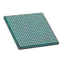
LFXP2-30E-5FN484C LATTICE SEMICONDUCTOR, LFXP2-30E-5FN484C Datasheet - Page 29

LFXP2-30E-5FN484C
Manufacturer Part Number
LFXP2-30E-5FN484C
Description
IC, LATTICEXP2 FPGA, 435MHZ, FPBGA-484
Manufacturer
LATTICE SEMICONDUCTOR
Series
LatticeXP2r
Datasheet
1.LFXP2-5E-5TN144C.pdf
(93 pages)
Specifications of LFXP2-30E-5FN484C
No. Of Logic Blocks
29000
No. Of Macrocells
14500
Family Type
LatticeXP2
No. Of Speed Grades
5
No. Of I/o's
363
Clock Management
PLL
Total Ram Bits
387Kbit
Lead Free Status / RoHS Status
Lead free / RoHS Compliant
Available stocks
Company
Part Number
Manufacturer
Quantity
Price
Company:
Part Number:
LFXP2-30E-5FN484C
Manufacturer:
Lattice Semiconductor Corporation
Quantity:
10 000
Lattice Semiconductor
Programmable I/O Cells (PIC)
Each PIC contains two PIOs connected to their respective sysIO buffers as shown in Figure 2-25. The PIO Block
supplies the output data (DO) and the tri-state control signal (TO) to the sysIO buffer and receives input from the
buffer. Table 2-11 provides the PIO signal list.
Figure 2-25. PIC Diagram
Two adjacent PIOs can be joined to provide a differential I/O pair (labeled as “T” and “C”) as shown in Figure 2-25.
The PAD Labels “T” and “C” distinguish the two PIOs. Approximately 50% of the PIO pairs on the left and right
edges of the device can be configured as true LVDS outputs. All I/O pairs can operate as inputs.
DDRCLKPOL
1. Signals are available on left/right/bottom edges only.
2. Selected blocks.
DQSXFER
ONEG2
QNEG0
QNEG1
OPOS2
QPOS0
QPOS1
OPOS1
ONEG1
OPOS0
ONEG0
ECLK1
ECLK2
IPOS0
IPOS1
GSRN
INCK
INDD
INFF
DQS
CLK
LSR
DEL
TD
CE
1
1
1
1
1
1
2
1
1
Control
Muxes
CLK1
CLK0
CEO
GSR
LSR
CEI
2-26
PIOA
Register
Register
Register
Tristate
Output
Block
Block
Block
Input
PIOB
IOLD0
IOLT0
DI
LatticeXP2 Family Data Sheet
Buffer
sysIO
PADB
PADA
“C”
“T”
Architecture


