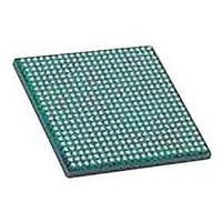
LFXP2-30E-5FN484C LATTICE SEMICONDUCTOR, LFXP2-30E-5FN484C Datasheet - Page 33

LFXP2-30E-5FN484C
Manufacturer Part Number
LFXP2-30E-5FN484C
Description
IC, LATTICEXP2 FPGA, 435MHZ, FPBGA-484
Manufacturer
LATTICE SEMICONDUCTOR
Series
LatticeXP2r
Datasheet
1.LFXP2-5E-5TN144C.pdf
(93 pages)
Specifications of LFXP2-30E-5FN484C
No. Of Logic Blocks
29000
No. Of Macrocells
14500
Family Type
LatticeXP2
No. Of Speed Grades
5
No. Of I/o's
363
Clock Management
PLL
Total Ram Bits
387Kbit
Lead Free Status / RoHS Status
Lead free / RoHS Compliant
Available stocks
Company
Part Number
Manufacturer
Quantity
Price
Company:
Part Number:
LFXP2-30E-5FN484C
Manufacturer:
Lattice Semiconductor Corporation
Quantity:
10 000
Architecture
Lattice Semiconductor
LatticeXP2 Family Data Sheet
Tristate Register Block
The tristate register block provides the ability to register tri-state control signals from the core of the device before
they are passed to the sysIO buffers. The block contains a register for SDR operation and an additional latch for
DDR operation. Figure 2-27 shows the Tristate Register Block with the Output Block
In SDR mode, ONEG1 feeds one of the flip-flops that then feeds the output. The flip-flop can be configured as D-
type or latch. In DDR mode, ONEG1 and OPOS1 are fed into registers on the positive edge of the clock. Then in
the next clock the registered OPOS1 is latched. A multiplexer running off the same clock cycle selects the correct
register for feeding to the output (D0).
Control Logic Block
The control logic block allows the selection and modification of control signals for use in the PIO block. A clock sig-
nal is selected from general purpose routing, ECLK1, ECLK2 or a DQS signal (from the programmable DQS pin)
and is provided to the input register block. The clock can optionally be inverted.
DDR Memory Support
PICs have additional circuitry to allow implementation of high speed source synchronous and DDR memory inter-
faces.
PICs have registered elements that support DDR memory interfaces. Interfaces on the left and right edges are
designed for DDR memories that support 16 bits of data, whereas interfaces on the top and bottom are designed
for memories that support 18 bits of data. One of every 16 PIOs on the left and right and one of every 18 PIOs on
the top and bottom contain delay elements to facilitate the generation of DQS signals. The DQS signals feed the
DQS buses which span the set of 16 or 18 PIOs. Figure 2-28 and Figure 2-29 show the DQS pin assignments in
each set of PIOs.
The exact DQS pins are shown in a dual function in the Logic Signal Connections table in this data sheet. Addi-
tional detail is provided in the Signal Descriptions table. The DQS signal from the bus is used to strobe the DDR
data from the memory into input register blocks. For additional information on using DDR memory support please
see TN1138, LatticeXP2 High Speed I/O Interface.
2-30


