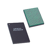
EP3C16F484A7N Altera, EP3C16F484A7N Datasheet - Page 117

EP3C16F484A7N
Manufacturer Part Number
EP3C16F484A7N
Description
Cyclone III
Manufacturer
Altera
Datasheet
1.EP3C16F484A7N.pdf
(274 pages)
Specifications of EP3C16F484A7N
Family Name
Cyclone III
Number Of Logic Blocks/elements
15408
# I/os (max)
346
Frequency (max)
437.5MHz
Process Technology
65nm
Operating Supply Voltage (typ)
1.2V
Logic Cells
15408
Ram Bits
516096
Operating Supply Voltage (min)
1.15V
Operating Supply Voltage (max)
1.25V
Operating Temp Range
-40C to 125C
Operating Temperature Classification
Automotive
Mounting
Surface Mount
Pin Count
484
Package Type
FBGA
Lead Free Status / Rohs Status
Compliant
Available stocks
Company
Part Number
Manufacturer
Quantity
Price
Company:
Part Number:
EP3C16F484A7N
Manufacturer:
ALTERA
Quantity:
717
Part Number:
EP3C16F484A7N
Manufacturer:
ALTERA/阿尔特拉
Quantity:
20 000
- Current page: 117 of 274
- Download datasheet (6Mb)
Chapter 6: I/O Features in the Cyclone III Device Family
I/O Banks
Table 6–5. Cyclone III Device Family I/O Standards Support
© December 2009
3.3-V LVTTL/LVCMOS,
3.0-V LVTTL/LVCMOS,
2.5-V LVTTL/LVCMOS,
1.8-V LVTTL/LVCMOS,
1.5-V LVCMOS,
1.2V LVCMOS,
3.0-V PCI / PCI-X
SSTL-18 Class I/II,
SSTL-2 Class I/II,
HSTL-18 Class I/II,
HSTL-15 Class I/II,
HSTL-12 Class I
HSTL-12 Class II
Differential SSTL-2,
Differential SSTL-18,
Differential HSTL-18,
Differential HSTL-15,
Differential HSTL-12
PPDS (2),
LVDS
BLVDS
RSDS and mini-LVDS
Differential LVPECL
Notes to
(1) These differential I/O standards are supported only for clock inputs and dedicated PLL_OUT outputs.
(2) True differential (PPDS, LVDS, mini-LVDS, and RSDS I/O standards) outputs are supported in row I/O banks only. Differential outputs in
(3) This I/O standard is supported for outputs only.
(4) This I/O standard is supported for clock inputs only.
column I/O banks require an external resistors network.
(2)
Table
(3)
6–5:
I/O Standard
Altera Corporation
(2)
Table 6–5
the I/O banks of the Cyclone III device family.
Each I/O bank of the Cyclone III device family has a VREF bus to accommodate
voltage-referenced I/O standards. Each VREF pin is the reference source for its V
group. If you use a V
VREF pin for that group to the appropriate voltage level. If you do not use all the V
groups in the I/O bank for voltage referenced I/O standards, you can use the VREF
pin in the unused voltage referenced groups as regular I/O pins. For example, if you
have SSTL-2 Class I input pins in I/O bank 1 and they are all placed in the VREFB1N0
group, VREFB1N0 must be powered with 1.25 V, and the remaining VREFB1N[1:3]
pins (if available) are used as I/O pins. If multiple V
I/O bank, the VREF pins must all be powered by the same voltage level because the
VREF pins are shorted together within the same I/O bank.
lists the I/O standards supported when a pin is used as a regular I/O pin in
(1)
(3)
(3)
(4)
v
v
v
v
—
1
REF
group for voltage-referenced I/O standards, connect the
v
v
(1)
(3)
v
v
(3)
(4)
—
2
(1)
(3)
(3)
(4)
v
v
v
v
v
3
(1)
(3)
(3)
(4)
v
v
v
v
v
4
I/O Banks
REF
(1)
(3)
(3)
(4)
v
v
v
v
—
5
groups are used in the same
Cyclone III Device Handbook, Volume 1
(1)
(3)
(3)
(4)
v
v
—
v
v
6
(1)
(3)
(3)
(4)
v
v
v
v
v
7
(1)
(3)
(3)
(4)
v
v
v
v
v
8
REF
6–17
REF
Related parts for EP3C16F484A7N
Image
Part Number
Description
Manufacturer
Datasheet
Request
R

Part Number:
Description:
CYCLONE II STARTER KIT EP2C20N
Manufacturer:
Altera
Datasheet:

Part Number:
Description:
CPLD, EP610 Family, ECMOS Process, 300 Gates, 16 Macro Cells, 16 Reg., 16 User I/Os, 5V Supply, 35 Speed Grade, 24DIP
Manufacturer:
Altera Corporation
Datasheet:

Part Number:
Description:
CPLD, EP610 Family, ECMOS Process, 300 Gates, 16 Macro Cells, 16 Reg., 16 User I/Os, 5V Supply, 15 Speed Grade, 24DIP
Manufacturer:
Altera Corporation
Datasheet:

Part Number:
Description:
Manufacturer:
Altera Corporation
Datasheet:

Part Number:
Description:
CPLD, EP610 Family, ECMOS Process, 300 Gates, 16 Macro Cells, 16 Reg., 16 User I/Os, 5V Supply, 30 Speed Grade, 24DIP
Manufacturer:
Altera Corporation
Datasheet:

Part Number:
Description:
High-performance, low-power erasable programmable logic devices with 8 macrocells, 10ns
Manufacturer:
Altera Corporation
Datasheet:

Part Number:
Description:
High-performance, low-power erasable programmable logic devices with 8 macrocells, 7ns
Manufacturer:
Altera Corporation
Datasheet:

Part Number:
Description:
Classic EPLD
Manufacturer:
Altera Corporation
Datasheet:

Part Number:
Description:
High-performance, low-power erasable programmable logic devices with 8 macrocells, 10ns
Manufacturer:
Altera Corporation
Datasheet:

Part Number:
Description:
Manufacturer:
Altera Corporation
Datasheet:

Part Number:
Description:
Manufacturer:
Altera Corporation
Datasheet:

Part Number:
Description:
Manufacturer:
Altera Corporation
Datasheet:

Part Number:
Description:
CPLD, EP610 Family, ECMOS Process, 300 Gates, 16 Macro Cells, 16 Reg., 16 User I/Os, 5V Supply, 25 Speed Grade, 24DIP
Manufacturer:
Altera Corporation
Datasheet:


