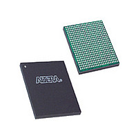
EP3C16F484A7N Altera, EP3C16F484A7N Datasheet - Page 120

EP3C16F484A7N
Manufacturer Part Number
EP3C16F484A7N
Description
Cyclone III
Manufacturer
Altera
Datasheet
1.EP3C16F484A7N.pdf
(274 pages)
Specifications of EP3C16F484A7N
Family Name
Cyclone III
Number Of Logic Blocks/elements
15408
# I/os (max)
346
Frequency (max)
437.5MHz
Process Technology
65nm
Operating Supply Voltage (typ)
1.2V
Logic Cells
15408
Ram Bits
516096
Operating Supply Voltage (min)
1.15V
Operating Supply Voltage (max)
1.25V
Operating Temp Range
-40C to 125C
Operating Temperature Classification
Automotive
Mounting
Surface Mount
Pin Count
484
Package Type
FBGA
Lead Free Status / Rohs Status
Compliant
Available stocks
Company
Part Number
Manufacturer
Quantity
Price
Company:
Part Number:
EP3C16F484A7N
Manufacturer:
ALTERA
Quantity:
717
Part Number:
EP3C16F484A7N
Manufacturer:
ALTERA/阿尔特拉
Quantity:
20 000
- Current page: 120 of 274
- Download datasheet (6Mb)
6–20
High-Speed Differential Interfaces
External Memory Interfacing
Cyclone III Device Handbook, Volume 1
f
f
f
For more information about the Cyclone III device family I/O interface with 3.3-, 3.0-,
or 2.5-V LVTTL/LVCMOS systems, refer to
3.3/3.0/2.5-V LVTTL/LVCMOS I/O
The Cyclone III device family can send and receive data through LVDS signals. For
the LVDS transmitter and receiver, the input and output pins of the Cyclone III device
family support serialization and deserialization through internal logic.
The BLVDS extends the benefits of LVDS to multipoint applications such as in
bidirectional backplanes. The loading effect and the need to terminate the bus at both
ends for multipoint applications require BLVDS to drive out a higher current than
LVDS to produce a comparable voltage swing. All the I/O banks of the Cyclone III
device family support BLVDS for user I/O pins.
The reduced swing differential signaling (RSDS) and mini-LVDS standards are
derivatives of the LVDS standard. The RSDS and mini-LVDS I/O standards are
similar in electrical characteristics to LVDS, but have a smaller voltage swing and
therefore provide increased power benefits and reduced electromagnetic interference
(EMI).
The point-to-point differential signaling (PPDS) standard is the next generation of the
RSDS standard introduced by National Semiconductor Corporation. The Cyclone III
device family meets the National Semiconductor Corporation PPDS Interface
Specification and supports the PPDS standard for outputs only. All the I/O banks of
the Cyclone III device family support the PPDS standard for output pins only.
You can use I/O pins and internal logic to implement the LVDS I/O receiver and
transmitter in the Cyclone III device family. Cyclone III and Cyclone III LS devices do
not contain dedicated serialization or deserialization circuitry. Therefore, shift
registers, internal PLLs, and IOEs are used to perform serial-to-parallel conversions
on incoming data and parallel-to-serial conversion on outgoing data.
The LVDS standard does not require an input reference voltage, but it does require a
100-Ω termination resistor between the two signals at the input buffer. An external
resistor network is required on the transmitter side for top and bottom I/O banks.
For more information about the Cyclone III device family high-speed differential
interface support, refer to the
chapter.
The Cyclone III device family supports I/O standards required to interface with a
broad range of external memory interfaces, such as DDR SDRAM, DDR2 SDRAM,
and QDRII SRAM.
For more information about the Cyclone III device family external memory interface
support, refer to the
External Memory Interfaces in Cyclone III Devices
High-Speed Differential Interfaces in Cyclone III Devices
Systems.
AN 447: Interfacing Cyclone III Devices with
Chapter 6: I/O Features in the Cyclone III Device Family
© December 2009 Altera Corporation
chapter.
I/O Banks
Related parts for EP3C16F484A7N
Image
Part Number
Description
Manufacturer
Datasheet
Request
R

Part Number:
Description:
CYCLONE II STARTER KIT EP2C20N
Manufacturer:
Altera
Datasheet:

Part Number:
Description:
CPLD, EP610 Family, ECMOS Process, 300 Gates, 16 Macro Cells, 16 Reg., 16 User I/Os, 5V Supply, 35 Speed Grade, 24DIP
Manufacturer:
Altera Corporation
Datasheet:

Part Number:
Description:
CPLD, EP610 Family, ECMOS Process, 300 Gates, 16 Macro Cells, 16 Reg., 16 User I/Os, 5V Supply, 15 Speed Grade, 24DIP
Manufacturer:
Altera Corporation
Datasheet:

Part Number:
Description:
Manufacturer:
Altera Corporation
Datasheet:

Part Number:
Description:
CPLD, EP610 Family, ECMOS Process, 300 Gates, 16 Macro Cells, 16 Reg., 16 User I/Os, 5V Supply, 30 Speed Grade, 24DIP
Manufacturer:
Altera Corporation
Datasheet:

Part Number:
Description:
High-performance, low-power erasable programmable logic devices with 8 macrocells, 10ns
Manufacturer:
Altera Corporation
Datasheet:

Part Number:
Description:
High-performance, low-power erasable programmable logic devices with 8 macrocells, 7ns
Manufacturer:
Altera Corporation
Datasheet:

Part Number:
Description:
Classic EPLD
Manufacturer:
Altera Corporation
Datasheet:

Part Number:
Description:
High-performance, low-power erasable programmable logic devices with 8 macrocells, 10ns
Manufacturer:
Altera Corporation
Datasheet:

Part Number:
Description:
Manufacturer:
Altera Corporation
Datasheet:

Part Number:
Description:
Manufacturer:
Altera Corporation
Datasheet:

Part Number:
Description:
Manufacturer:
Altera Corporation
Datasheet:

Part Number:
Description:
CPLD, EP610 Family, ECMOS Process, 300 Gates, 16 Macro Cells, 16 Reg., 16 User I/Os, 5V Supply, 25 Speed Grade, 24DIP
Manufacturer:
Altera Corporation
Datasheet:


