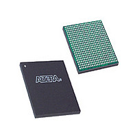
EP3C16F484A7N Altera, EP3C16F484A7N Datasheet - Page 68

EP3C16F484A7N
Manufacturer Part Number
EP3C16F484A7N
Description
Cyclone III
Manufacturer
Altera
Datasheet
1.EP3C16F484A7N.pdf
(274 pages)
Specifications of EP3C16F484A7N
Family Name
Cyclone III
Number Of Logic Blocks/elements
15408
# I/os (max)
346
Frequency (max)
437.5MHz
Process Technology
65nm
Operating Supply Voltage (typ)
1.2V
Logic Cells
15408
Ram Bits
516096
Operating Supply Voltage (min)
1.15V
Operating Supply Voltage (max)
1.25V
Operating Temp Range
-40C to 125C
Operating Temperature Classification
Automotive
Mounting
Surface Mount
Pin Count
484
Package Type
FBGA
Lead Free Status / Rohs Status
Compliant
Available stocks
Company
Part Number
Manufacturer
Quantity
Price
Company:
Part Number:
EP3C16F484A7N
Manufacturer:
ALTERA
Quantity:
717
Part Number:
EP3C16F484A7N
Manufacturer:
ALTERA/阿尔特拉
Quantity:
20 000
- Current page: 68 of 274
- Download datasheet (6Mb)
5–4
Clock Control Block
Cyclone III Device Handbook, Volume 1
f
If you do not use dedicated clock pins to feed the GCLKs, you can use them as
general-purpose input pins to feed the logic array. However, when using them as
general-purpose input pins, they do not have support for an I/O register and must
use LE-based registers in place of an I/O register.
For more information about how to connect the clock and PLL pins, refer to the
Cyclone III Device Family Pin Connection Guidelines
The clock control block drives GCLKs. Clock control blocks are located on each side of
the device, close to the dedicated clock input pins. GCLKs are optimized for
minimum clock skew and delay.
Table 5–2
GCLKs.
Table 5–2. Clock Control Block Inputs
In the Cyclone III device family, dedicated clock input pins, PLL counter outputs,
dual-purpose clock I/O inputs, and internal logic can all feed the clock control block
for each GCLK. The output from the clock control block in turn feeds the
corresponding GCLK. The GCLK can drive the PLL input if the clock control block
inputs are outputs of another PLL or dedicated clock input pins. The clock control
blocks are at the device periphery; there are a maximum of 20 clock control blocks
available per Cyclone III device family.
The control block has two functions:
■
■
Dedicated clock inputs
Dual-purpose clock
(DPCLK and CDPCLK)
I/O input
PLL outputs
Internal logic
Dynamic GCLK clock source selection (not applicable for DPCLK or CDPCLK and
internal logic input)
GCLK network power down (dynamic enable and disable)
lists the sources that can feed the clock control block, which in turn feeds the
Input
Dedicated clock input pins can drive clocks or global signals, such as
synchronous and asynchronous clears, presets, or clock enables onto
given GCLKs.
DPCLK and CDPCLK I/O pins are bidirectional dual function pins that
are used for high fan-out control signals, such as protocol signals,
TRDY and IRDY signals for PCI, via the GCLK. Clock control blocks
that have inputs driven by dual-purpose clock I/O pins are not able to
drive PLL inputs.
PLL counter outputs can drive the GCLK.
You can drive the GCLK through logic array routing to enable internal
logic elements (LEs) to drive a high fan-out, low-skew signal path.
Clock control blocks that have inputs driven by internal logic are not
able to drive PLL inputs.
Chapter 5: Clock Networks and PLLs in the Cyclone III Device Family
on the Altera
Description
© December 2009 Altera Corporation
®
website.
Clock Networks
Related parts for EP3C16F484A7N
Image
Part Number
Description
Manufacturer
Datasheet
Request
R

Part Number:
Description:
CYCLONE II STARTER KIT EP2C20N
Manufacturer:
Altera
Datasheet:

Part Number:
Description:
CPLD, EP610 Family, ECMOS Process, 300 Gates, 16 Macro Cells, 16 Reg., 16 User I/Os, 5V Supply, 35 Speed Grade, 24DIP
Manufacturer:
Altera Corporation
Datasheet:

Part Number:
Description:
CPLD, EP610 Family, ECMOS Process, 300 Gates, 16 Macro Cells, 16 Reg., 16 User I/Os, 5V Supply, 15 Speed Grade, 24DIP
Manufacturer:
Altera Corporation
Datasheet:

Part Number:
Description:
Manufacturer:
Altera Corporation
Datasheet:

Part Number:
Description:
CPLD, EP610 Family, ECMOS Process, 300 Gates, 16 Macro Cells, 16 Reg., 16 User I/Os, 5V Supply, 30 Speed Grade, 24DIP
Manufacturer:
Altera Corporation
Datasheet:

Part Number:
Description:
High-performance, low-power erasable programmable logic devices with 8 macrocells, 10ns
Manufacturer:
Altera Corporation
Datasheet:

Part Number:
Description:
High-performance, low-power erasable programmable logic devices with 8 macrocells, 7ns
Manufacturer:
Altera Corporation
Datasheet:

Part Number:
Description:
Classic EPLD
Manufacturer:
Altera Corporation
Datasheet:

Part Number:
Description:
High-performance, low-power erasable programmable logic devices with 8 macrocells, 10ns
Manufacturer:
Altera Corporation
Datasheet:

Part Number:
Description:
Manufacturer:
Altera Corporation
Datasheet:

Part Number:
Description:
Manufacturer:
Altera Corporation
Datasheet:

Part Number:
Description:
Manufacturer:
Altera Corporation
Datasheet:

Part Number:
Description:
CPLD, EP610 Family, ECMOS Process, 300 Gates, 16 Macro Cells, 16 Reg., 16 User I/Os, 5V Supply, 25 Speed Grade, 24DIP
Manufacturer:
Altera Corporation
Datasheet:


