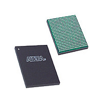
EP3C16F484A7N Altera, EP3C16F484A7N Datasheet - Page 82

EP3C16F484A7N
Manufacturer Part Number
EP3C16F484A7N
Description
Cyclone III
Manufacturer
Altera
Datasheet
1.EP3C16F484A7N.pdf
(274 pages)
Specifications of EP3C16F484A7N
Family Name
Cyclone III
Number Of Logic Blocks/elements
15408
# I/os (max)
346
Frequency (max)
437.5MHz
Process Technology
65nm
Operating Supply Voltage (typ)
1.2V
Logic Cells
15408
Ram Bits
516096
Operating Supply Voltage (min)
1.15V
Operating Supply Voltage (max)
1.25V
Operating Temp Range
-40C to 125C
Operating Temperature Classification
Automotive
Mounting
Surface Mount
Pin Count
484
Package Type
FBGA
Lead Free Status / Rohs Status
Compliant
Available stocks
Company
Part Number
Manufacturer
Quantity
Price
Company:
Part Number:
EP3C16F484A7N
Manufacturer:
ALTERA
Quantity:
717
Part Number:
EP3C16F484A7N
Manufacturer:
ALTERA/阿尔特拉
Quantity:
20 000
- Current page: 82 of 274
- Download datasheet (6Mb)
5–18
Clock Switchover
Cyclone III Device Handbook, Volume 1
f
If you use the SignalTap
locked signal goes low only when areset is deasserted. If the areset signal is not
enabled, the extra logic is not implemented in the ALTPLL megafunction.
For more information about the PLL control signals, refer to the
User
The clock switchover feature allows the PLL to switch between two reference input
clocks. Use this feature for clock redundancy or for a dual-clock domain application,
such as a system that turns on the redundant clock if the previous clock stops
running. Your design can automatically perform clock switchover when the clock is
no longer toggling, or based on the user control signal, clkswitch.
Automatic Clock Switchover
Cyclone III device family PLLs support a fully configurable clock switchover
capability.
When the current reference clock is not present, the clock-sense block automatically
switches to the backup clock for PLL reference. The clock switchover circuit also
sends out three status signals—clkbad[0], clkbad[1], and activeclock—from
the PLL to implement a custom switchover circuit. You can select a clock source at the
backup clock by connecting it to the inclk1 port of the PLL in your design.
Figure 5–14
Figure 5–14. Automatic Clock Switchover Circuit
Guide.
inclk1
inclk0
shows the block diagram of the switchover circuit built into the PLL.
muxout
®
II tool to probe the locked signal before the D flip-flop, the
clksw
n Counter
Sense
Clock
Chapter 5: Clock Networks and PLLs in the Cyclone III Device Family
refclk
Switchover
Machine
State
© December 2009 Altera Corporation
PFD
ALTPLL Megafunction
clkswitch
(provides manual
switchover support)
fbclk
clkbad0
clkbad1
Activeclock
Hardware Features
Related parts for EP3C16F484A7N
Image
Part Number
Description
Manufacturer
Datasheet
Request
R

Part Number:
Description:
CYCLONE II STARTER KIT EP2C20N
Manufacturer:
Altera
Datasheet:

Part Number:
Description:
CPLD, EP610 Family, ECMOS Process, 300 Gates, 16 Macro Cells, 16 Reg., 16 User I/Os, 5V Supply, 35 Speed Grade, 24DIP
Manufacturer:
Altera Corporation
Datasheet:

Part Number:
Description:
CPLD, EP610 Family, ECMOS Process, 300 Gates, 16 Macro Cells, 16 Reg., 16 User I/Os, 5V Supply, 15 Speed Grade, 24DIP
Manufacturer:
Altera Corporation
Datasheet:

Part Number:
Description:
Manufacturer:
Altera Corporation
Datasheet:

Part Number:
Description:
CPLD, EP610 Family, ECMOS Process, 300 Gates, 16 Macro Cells, 16 Reg., 16 User I/Os, 5V Supply, 30 Speed Grade, 24DIP
Manufacturer:
Altera Corporation
Datasheet:

Part Number:
Description:
High-performance, low-power erasable programmable logic devices with 8 macrocells, 10ns
Manufacturer:
Altera Corporation
Datasheet:

Part Number:
Description:
High-performance, low-power erasable programmable logic devices with 8 macrocells, 7ns
Manufacturer:
Altera Corporation
Datasheet:

Part Number:
Description:
Classic EPLD
Manufacturer:
Altera Corporation
Datasheet:

Part Number:
Description:
High-performance, low-power erasable programmable logic devices with 8 macrocells, 10ns
Manufacturer:
Altera Corporation
Datasheet:

Part Number:
Description:
Manufacturer:
Altera Corporation
Datasheet:

Part Number:
Description:
Manufacturer:
Altera Corporation
Datasheet:

Part Number:
Description:
Manufacturer:
Altera Corporation
Datasheet:

Part Number:
Description:
CPLD, EP610 Family, ECMOS Process, 300 Gates, 16 Macro Cells, 16 Reg., 16 User I/Os, 5V Supply, 25 Speed Grade, 24DIP
Manufacturer:
Altera Corporation
Datasheet:


