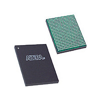
EP3C16F484A7N Altera, EP3C16F484A7N Datasheet - Page 208

EP3C16F484A7N
Manufacturer Part Number
EP3C16F484A7N
Description
Cyclone III
Manufacturer
Altera
Datasheet
1.EP3C16F484A7N.pdf
(274 pages)
Specifications of EP3C16F484A7N
Family Name
Cyclone III
Number Of Logic Blocks/elements
15408
# I/os (max)
346
Frequency (max)
437.5MHz
Process Technology
65nm
Operating Supply Voltage (typ)
1.2V
Logic Cells
15408
Ram Bits
516096
Operating Supply Voltage (min)
1.15V
Operating Supply Voltage (max)
1.25V
Operating Temp Range
-40C to 125C
Operating Temperature Classification
Automotive
Mounting
Surface Mount
Pin Count
484
Package Type
FBGA
Lead Free Status / Rohs Status
Compliant
Available stocks
Company
Part Number
Manufacturer
Quantity
Price
Company:
Part Number:
EP3C16F484A7N
Manufacturer:
ALTERA
Quantity:
717
Part Number:
EP3C16F484A7N
Manufacturer:
ALTERA/阿尔特拉
Quantity:
20 000
- Current page: 208 of 274
- Download datasheet (6Mb)
9–48
Table 9–14. FPP Timing Parameters for Cyclone III Device Family
JTAG Configuration
Cyclone III Device Handbook, Volume 1
t
t
Notes to
(1) This information is preliminary.
(2) This value is applicable if users do not delay configuration by extending the nCONFIG or nSTATUS low pulse width.
(3) The minimum and maximum numbers apply only if the internal oscillator is chosen as the clock source for starting up the device.
(4) Cyclone III EP3C5, EP3C10, EP3C16, EP3C25, and EP3C40 devices support a DCLK f
(5) For more information about the initialization clock cycles required in Cyclone III device family, refer to
CD2C U
CD2UM C
Symbol
and all the Cyclone III LS devices support a DCLK f
Table
f
9–14:
1
CONF_DONE high to CLKUSR enabled
CONF_DONE high to user mode with CLKUSR
option on
JTAG has developed a specification for boundary-scan testing. This boundary-scan
test (BST) architecture offers the capability to efficiently test components on PCBs
with tight lead spacing. The BST architecture can test pin connections without using
physical test probes and capture functional data while a device is operating normally.
You can also use the JTAG circuitry to shift configuration data into the device. The
Quartus II software automatically generates .sofs that are used for JTAG
configuration with a download cable in the Quartus II software programmer.
For more information about JTAG boundary-scan testing, refer to the
(JTAG) Boundary-Scan Testing for Cyclone III Devices
JTAG instructions have precedence over any other device configuration modes.
Therefore, JTAG configuration can take place without waiting for other configuration
modes to complete. For example, if you attempt JTAG configuration of Cyclone III
device family during PS configuration, PS configuration terminates and JTAG
configuration begins. If the Cyclone III device family MSEL pins are set to AS mode,
the Cyclone III device family does not output a DCLK signal when JTAG configuration
takes place.
The four required pins for a device operating in JTAG mode are TDI, TDO, TMS, and
TCK. The TCK pin has an internal weak pull-down resistor while the TDI and TMS pins
have weak internal pull-up resistors (typically 25 kΩ). The TDO output pin is powered
by V
JTAG pins support only LVTTL I/O standard. All user I/O pins are tri-stated during
JTAG configuration.
The TDO output is powered by the V
CCIO
Chapter 9: Configuration, Design Security, and Remote System Upgrades in the Cyclone III Device Family
in I/O bank 1. All the JTAG input pins are powered by the V
Parameter
MAX
Table 9–15
of 100 MHz.
lists the function of each JTAG pin.
CCIO
(Note 1)
4 × maximum DCLK period
t
cycles × CLKUSR period)
C D2CU
power supply of I/O bank 1.
+ (initialization clock
MAX
Minimum
(Part 2 of 2)
of 133 MHz. Cyclone III EP3C55, EP3C80, EP3C120
chapter.
Table 9–5 on page
© December 2009 Altera Corporation
(5)
Maximum
CCIO
Configuration Features
IEEE 1149.1
9–10.
—
—
pin. All the
Unit
—
—
Related parts for EP3C16F484A7N
Image
Part Number
Description
Manufacturer
Datasheet
Request
R

Part Number:
Description:
CYCLONE II STARTER KIT EP2C20N
Manufacturer:
Altera
Datasheet:

Part Number:
Description:
CPLD, EP610 Family, ECMOS Process, 300 Gates, 16 Macro Cells, 16 Reg., 16 User I/Os, 5V Supply, 35 Speed Grade, 24DIP
Manufacturer:
Altera Corporation
Datasheet:

Part Number:
Description:
CPLD, EP610 Family, ECMOS Process, 300 Gates, 16 Macro Cells, 16 Reg., 16 User I/Os, 5V Supply, 15 Speed Grade, 24DIP
Manufacturer:
Altera Corporation
Datasheet:

Part Number:
Description:
Manufacturer:
Altera Corporation
Datasheet:

Part Number:
Description:
CPLD, EP610 Family, ECMOS Process, 300 Gates, 16 Macro Cells, 16 Reg., 16 User I/Os, 5V Supply, 30 Speed Grade, 24DIP
Manufacturer:
Altera Corporation
Datasheet:

Part Number:
Description:
High-performance, low-power erasable programmable logic devices with 8 macrocells, 10ns
Manufacturer:
Altera Corporation
Datasheet:

Part Number:
Description:
High-performance, low-power erasable programmable logic devices with 8 macrocells, 7ns
Manufacturer:
Altera Corporation
Datasheet:

Part Number:
Description:
Classic EPLD
Manufacturer:
Altera Corporation
Datasheet:

Part Number:
Description:
High-performance, low-power erasable programmable logic devices with 8 macrocells, 10ns
Manufacturer:
Altera Corporation
Datasheet:

Part Number:
Description:
Manufacturer:
Altera Corporation
Datasheet:

Part Number:
Description:
Manufacturer:
Altera Corporation
Datasheet:

Part Number:
Description:
Manufacturer:
Altera Corporation
Datasheet:

Part Number:
Description:
CPLD, EP610 Family, ECMOS Process, 300 Gates, 16 Macro Cells, 16 Reg., 16 User I/Os, 5V Supply, 25 Speed Grade, 24DIP
Manufacturer:
Altera Corporation
Datasheet:


