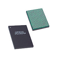
EP3C16F484A7N Altera, EP3C16F484A7N Datasheet - Page 152

EP3C16F484A7N
Manufacturer Part Number
EP3C16F484A7N
Description
Cyclone III
Manufacturer
Altera
Datasheet
1.EP3C16F484A7N.pdf
(274 pages)
Specifications of EP3C16F484A7N
Family Name
Cyclone III
Number Of Logic Blocks/elements
15408
# I/os (max)
346
Frequency (max)
437.5MHz
Process Technology
65nm
Operating Supply Voltage (typ)
1.2V
Logic Cells
15408
Ram Bits
516096
Operating Supply Voltage (min)
1.15V
Operating Supply Voltage (max)
1.25V
Operating Temp Range
-40C to 125C
Operating Temperature Classification
Automotive
Mounting
Surface Mount
Pin Count
484
Package Type
FBGA
Lead Free Status / Rohs Status
Compliant
Available stocks
Company
Part Number
Manufacturer
Quantity
Price
Company:
Part Number:
EP3C16F484A7N
Manufacturer:
ALTERA
Quantity:
717
Part Number:
EP3C16F484A7N
Manufacturer:
ALTERA/阿尔特拉
Quantity:
20 000
- Current page: 152 of 274
- Download datasheet (6Mb)
8–8
Figure 8–2. DQS, CQ, or CQ# Pins in Cyclone III Device Family I/O Banks
Note to
(1) The DQS, CQ, or CQ# pin locations in this diagram apply to all packages in Cyclone III device family except devices in 144-pin EQFP and 164-pin
Cyclone III Device Handbook, Volume 1
MBGA.
Figure
8–2:
1
1
Each DQ group is associated with its corresponding DQS pins, as defined in the
Cyclone III and Cyclone III LS pin tables; for example:
The Quartus
with its associated DQS.
Figure 8–2
Cyclone III device family I/O banks.
For Cyclone III device family memory interface support, only one interface is placed
on each side.
■
■
DQS1L/CQ1L#
DQS3L/CQ3L#
For DDR2 or DDR SDRAM, ×8 DQ group DQ3B[7:0] pins are associated with
the DQS3B pin (same 3B group index)
For QDR II SRAM, ×9 Q read-data group DQ3L[8..0] pins are associated
with DQS2L/CQ3L and DQS3L/CQ3L# pins (same 3L group index)
DQS2L/CQ3L
DQS0L/CQ1L
shows the location and numbering of the DQS, DQ, or CQ# pins in the
®
II software issues an error message if a DQ group is not placed properly
I/O Bank 3
I/O Bank 8
Cyclone III Device Family
Chapter 8: External Memory Interfaces in the Cyclone III Device Family
I/O Bank 7
I/O Bank 4
(Note 1)
Cyclone III Device Family Memory Interfaces Pin Support
DQS3R/CQ3R#
DQS0R/CQ1R
DQS1R/CQ1R#
DQS2R/CQ3R
© January 2010 Altera Corporation
Related parts for EP3C16F484A7N
Image
Part Number
Description
Manufacturer
Datasheet
Request
R

Part Number:
Description:
CYCLONE II STARTER KIT EP2C20N
Manufacturer:
Altera
Datasheet:

Part Number:
Description:
CPLD, EP610 Family, ECMOS Process, 300 Gates, 16 Macro Cells, 16 Reg., 16 User I/Os, 5V Supply, 35 Speed Grade, 24DIP
Manufacturer:
Altera Corporation
Datasheet:

Part Number:
Description:
CPLD, EP610 Family, ECMOS Process, 300 Gates, 16 Macro Cells, 16 Reg., 16 User I/Os, 5V Supply, 15 Speed Grade, 24DIP
Manufacturer:
Altera Corporation
Datasheet:

Part Number:
Description:
Manufacturer:
Altera Corporation
Datasheet:

Part Number:
Description:
CPLD, EP610 Family, ECMOS Process, 300 Gates, 16 Macro Cells, 16 Reg., 16 User I/Os, 5V Supply, 30 Speed Grade, 24DIP
Manufacturer:
Altera Corporation
Datasheet:

Part Number:
Description:
High-performance, low-power erasable programmable logic devices with 8 macrocells, 10ns
Manufacturer:
Altera Corporation
Datasheet:

Part Number:
Description:
High-performance, low-power erasable programmable logic devices with 8 macrocells, 7ns
Manufacturer:
Altera Corporation
Datasheet:

Part Number:
Description:
Classic EPLD
Manufacturer:
Altera Corporation
Datasheet:

Part Number:
Description:
High-performance, low-power erasable programmable logic devices with 8 macrocells, 10ns
Manufacturer:
Altera Corporation
Datasheet:

Part Number:
Description:
Manufacturer:
Altera Corporation
Datasheet:

Part Number:
Description:
Manufacturer:
Altera Corporation
Datasheet:

Part Number:
Description:
Manufacturer:
Altera Corporation
Datasheet:

Part Number:
Description:
CPLD, EP610 Family, ECMOS Process, 300 Gates, 16 Macro Cells, 16 Reg., 16 User I/Os, 5V Supply, 25 Speed Grade, 24DIP
Manufacturer:
Altera Corporation
Datasheet:


