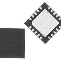
C8051F336-GMR Silicon Laboratories Inc, C8051F336-GMR Datasheet - Page 119

C8051F336-GMR
Manufacturer Part Number
C8051F336-GMR
Description
Microcontrollers (MCU) 16KB 10ADC 10DAC 768Ram MCU Lead Free
Manufacturer
Silicon Laboratories Inc
Datasheet
1.C8051F336-GM.pdf
(226 pages)
Specifications of C8051F336-GMR
Processor Series
C8051F3x
Core
8051
Data Bus Width
8 bit
Program Memory Type
Flash
Program Memory Size
16 KB
Data Ram Size
768 B
Interface Type
I2C, SPI, UART
Maximum Clock Frequency
25 MHz
Number Of Programmable I/os
17
Number Of Timers
4
Operating Supply Voltage
2.7 V to 3.6 V
Maximum Operating Temperature
+ 85 C
Mounting Style
SMD/SMT
Package / Case
QFN-20
3rd Party Development Tools
KSK-SL-TOOLSTICK, PK51, CA51, A51, ULINK2
Development Tools By Supplier
C8051F336DK
Minimum Operating Temperature
- 40 C
On-chip Adc
10 bit
On-chip Dac
10 bit
Package
20QFN
Device Core
8051
Family Name
C8051F336
Maximum Speed
25 MHz
Ram Size
768 Byte
Operating Temperature
-40 to 85 °C
Lead Free Status / Rohs Status
Details
Available stocks
Company
Part Number
Manufacturer
Quantity
Price
Company:
Part Number:
C8051F336-GMR
Manufacturer:
SILICON
Quantity:
100
Part Number:
C8051F336-GMR
Manufacturer:
SILICON LABS/芯科
Quantity:
20 000
Company:
Part Number:
C8051F336-GMR
Manufacturer:
SILICON
Quantity:
13 282
20. Port Input/Output
Digital and analog resources are available through 17 (C8051F336/7) or 21 (C8051F338/9) I/O pins. Port
pins P0.0-P2.3 can be defined as general-purpose I/O (GPIO), assigned to one of the internal digital
resources, or assigned to an analog function as shown in Figure 20.4. Port pin P2.4 on the C8051F338/9
and P2.0 on the C8051F336/7 can be used as GPIO and are shared with the C2 Interface Data signal
(C2D). The designer has complete control over which functions are assigned, limited only by the number of
physical I/O pins. This resource assignment flexibility is achieved through the use of a Priority Crossbar
Decoder. Note that the state of a Port I/O pin can always be read in the corresponding Port latch, regard-
less of the Crossbar settings.
The Crossbar assigns the selected internal digital resources to the I/O pins based on the Priority Decoder
(Figure 20.4 and Figure 20.5). The registers XBR0 and XBR1, defined in SFR Definition 20.1 and SFR
Definition 20.2, are used to select internal digital functions.
All Port I/Os are 5 V tolerant (refer to Figure 20.2 for the Port cell circuit). The Port I/O cells are configured
as either push-pull or open-drain in the Port Output Mode registers (PnMDOUT, where n = 0,1). Complete
Electrical Specifications for Port I/O are given in
Highest
Priority
Lowest
Priority
SYSCLK
Outputs
SMBus
T0, T1
UART
P0
P1
P2
PCA
CP0
SPI
(P0.0-P0.7)
(P1.0-P1.7)
(P2.0-P2.3*)
Figure 20.1. Port I/O Functional Block Diagram
2
4
2
2
4
2
8
8
4
PnSKIP Registers
XBR0, XBR1,
Crossbar
Decoder
Priority
Digital
Section “6. Electrical Characteristics” on page
Rev.1.0
(ADC0, CP0, VREF, XTAL)
To Analog Peripherals
8
8
4
P0MASK, P0MAT
P1MASK, P1MAT
Port Match
Cells
Cells
Cell
I/O
I/O
I/O
P0
P1
P2
C8051F336/7/8/9
External Interrupts
PnMDIN Registers
EX0 and EX1
PnMDOUT,
*P2.0-P2.3 are only available through
the crossbar on QFN24 Packages.
P0.0
P0.7
P1.0
P1.7
P2.0*
P2.3*
27.
119


