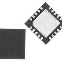
C8051F336-GMR Silicon Laboratories Inc, C8051F336-GMR Datasheet - Page 89

C8051F336-GMR
Manufacturer Part Number
C8051F336-GMR
Description
Microcontrollers (MCU) 16KB 10ADC 10DAC 768Ram MCU Lead Free
Manufacturer
Silicon Laboratories Inc
Datasheet
1.C8051F336-GM.pdf
(226 pages)
Specifications of C8051F336-GMR
Processor Series
C8051F3x
Core
8051
Data Bus Width
8 bit
Program Memory Type
Flash
Program Memory Size
16 KB
Data Ram Size
768 B
Interface Type
I2C, SPI, UART
Maximum Clock Frequency
25 MHz
Number Of Programmable I/os
17
Number Of Timers
4
Operating Supply Voltage
2.7 V to 3.6 V
Maximum Operating Temperature
+ 85 C
Mounting Style
SMD/SMT
Package / Case
QFN-20
3rd Party Development Tools
KSK-SL-TOOLSTICK, PK51, CA51, A51, ULINK2
Development Tools By Supplier
C8051F336DK
Minimum Operating Temperature
- 40 C
On-chip Adc
10 bit
On-chip Dac
10 bit
Package
20QFN
Device Core
8051
Family Name
C8051F336
Maximum Speed
25 MHz
Ram Size
768 Byte
Operating Temperature
-40 to 85 °C
Lead Free Status / Rohs Status
Details
Available stocks
Company
Part Number
Manufacturer
Quantity
Price
Company:
Part Number:
C8051F336-GMR
Manufacturer:
SILICON
Quantity:
100
Part Number:
C8051F336-GMR
Manufacturer:
SILICON LABS/芯科
Quantity:
20 000
Company:
Part Number:
C8051F336-GMR
Manufacturer:
SILICON
Quantity:
13 282
15.3. External Interrupts /INT0 and /INT1
The /INT0 and /INT1 external interrupt sources are configurable as active high or low, edge or level sensi-
tive. The IN0PL (/INT0 Polarity) and IN1PL (/INT1 Polarity) bits in the IT01CF register select active high or
active low; the IT0 and IT1 bits in TCON
or edge sensitive. The table below lists the possible configurations.
/INT0 and /INT1 are assigned to Port pins as defined in the IT01CF register (see SFR Definition 15.5).
Note that /INT0 and /INT0 Port pin assignments are independent of any Crossbar assignments. /INT0 and
/INT1 will monitor their assigned Port pins without disturbing the peripheral that was assigned the Port pin
via the Crossbar. To assign a Port pin only to /INT0 and/or /INT1, configure the Crossbar to skip the
selected pin(s). This is accomplished by setting the associated bit in register XBR0 (see
“20.3. Priority Crossbar Decoder” on page 124
IE0 (TCON.1) and IE1 (TCON.3) serve as the interrupt-pending flags for the /INT0 and /INT1 external
interrupts, respectively. If an /INT0 or /INT1 external interrupt is configured as edge-sensitive, the corre-
sponding interrupt-pending flag is automatically cleared by the hardware when the CPU vectors to the ISR.
When configured as level sensitive, the interrupt-pending flag remains logic 1 while the input is active as
defined by the corresponding polarity bit (IN0PL or IN1PL); the flag remains logic 0 while the input is inac-
tive. The external interrupt source must hold the input active until the interrupt request is recognized. It
must then deactivate the interrupt request before execution of the ISR completes or another interrupt
request will be generated.
IT0
1
1
0
0
IN0PL
0
1
0
1
Active low, edge sensitive
Active high, edge sensitive
Active low, level sensitive
Active high, level sensitive
/INT0 Interrupt
(Section “24.1. Timer 0 and Timer 1” on page
Rev.1.0
for complete details on configuring the Crossbar).
IT1
1
0
0
1
IN1PL
C8051F336/7/8/9
0
1
0
1
Active high, edge sensitive
Active low, level sensitive
Active high, level sensitive
Active low, edge sensitive
/INT1 Interrupt
182) select level
Section
89


