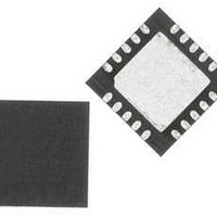
C8051F336-GMR Silicon Laboratories Inc, C8051F336-GMR Datasheet - Page 209

C8051F336-GMR
Manufacturer Part Number
C8051F336-GMR
Description
Microcontrollers (MCU) 16KB 10ADC 10DAC 768Ram MCU Lead Free
Manufacturer
Silicon Laboratories Inc
Datasheet
1.C8051F336-GM.pdf
(226 pages)
Specifications of C8051F336-GMR
Processor Series
C8051F3x
Core
8051
Data Bus Width
8 bit
Program Memory Type
Flash
Program Memory Size
16 KB
Data Ram Size
768 B
Interface Type
I2C, SPI, UART
Maximum Clock Frequency
25 MHz
Number Of Programmable I/os
17
Number Of Timers
4
Operating Supply Voltage
2.7 V to 3.6 V
Maximum Operating Temperature
+ 85 C
Mounting Style
SMD/SMT
Package / Case
QFN-20
3rd Party Development Tools
KSK-SL-TOOLSTICK, PK51, CA51, A51, ULINK2
Development Tools By Supplier
C8051F336DK
Minimum Operating Temperature
- 40 C
On-chip Adc
10 bit
On-chip Dac
10 bit
Package
20QFN
Device Core
8051
Family Name
C8051F336
Maximum Speed
25 MHz
Ram Size
768 Byte
Operating Temperature
-40 to 85 °C
Lead Free Status / Rohs Status
Details
Available stocks
Company
Part Number
Manufacturer
Quantity
Price
Company:
Part Number:
C8051F336-GMR
Manufacturer:
SILICON
Quantity:
100
Part Number:
C8051F336-GMR
Manufacturer:
SILICON LABS/芯科
Quantity:
20 000
25.3.4. Frequency Output Mode
Frequency Output Mode produces a programmable-frequency square wave on the module’s associated
CEXn pin. The capture/compare module high byte holds the number of PCA clocks to count before the out-
put is toggled. The frequency of the square wave is then defined by Equation 25.1.
Where F
PCA0MD. The lower byte of the capture/compare module is compared to the PCA counter low byte; on a
match, CEXn is toggled and the offset held in the high byte is added to the matched value in PCA0CPLn.
Frequency Output Mode is enabled by setting the ECOMn, TOGn, and PWMn bits in the PCA0CPMn reg-
ister. Note that the MATn bit should normally be set to 0 in this mode. If the MATn bit is set to 1, the CCFn
flag for the channel will be set when the 16-bit PCA0 counter and the 16-bit capture/compare register for
the channel are equal.
25.3.5. 8-bit, 9-bit, 10-bit and 11-bit Pulse Width Modulator Modes
Each module can be used independently to generate a pulse width modulated (PWM) output on its associ-
ated CEXn pin. The frequency of the output is dependent on the timebase for the PCA counter/timer, and
the setting of the PWM cycle length (8, 9, 10 or 11-bits). For backwards-compatibility with the 8-bit PWM
mode available on other devices, the 8-bit PWM mode operates slightly different than 9, 10 and 11-bit
PWM modes. It is important to note that all channels configured for 8/9/10/11-bit PWM mode will use
the same cycle length. It is not possible to configure one channel for 8-bit PWM mode and another for 11-
bit mode (for example). However, other PCA channels can be configured to Pin Capture, High-Speed Out-
put, Software Timer, Frequency Output, or 16-bit PWM mode independently.
Note: A value of 0x00 in the PCA0CPHn register is equal to 256 for this equation.
PCA0CPLn
Write to
Reset
PCA0CPHn
PCA
Write to
is the frequency of the clock selected by the CPS2–0 bits in the PCA mode register,
0
ENB
ENB
1
Equation 25.1. Square Wave Frequency Output
W
M
P
1
6
n
Figure 25.7. PCA Frequency Output Mode
x
C
O
M
E
n
PCA0CPMn
C
A
P
P
n
0 0 0
C
A
P
N
n
M
A
T
n
T
O
G
n
W
M
P
n
C
C
E
F
n
x
PCA Timebase
F
CEXn
Enable
=
---------------------------------------- -
2
Comparator
PCA0CPLn
Rev.1.0
PCA0L
×
8-bit
PCA0CPHn
F
PCA
match
Enable
Adder
8-bit Adder
Toggle
C8051F336/7/8/9
TOGn
0
1
CEXn
PCA0CPHn
Crossbar
Port I/O
209


