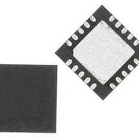
C8051F336-GMR Silicon Laboratories Inc, C8051F336-GMR Datasheet - Page 124

C8051F336-GMR
Manufacturer Part Number
C8051F336-GMR
Description
Microcontrollers (MCU) 16KB 10ADC 10DAC 768Ram MCU Lead Free
Manufacturer
Silicon Laboratories Inc
Datasheet
1.C8051F336-GM.pdf
(226 pages)
Specifications of C8051F336-GMR
Processor Series
C8051F3x
Core
8051
Data Bus Width
8 bit
Program Memory Type
Flash
Program Memory Size
16 KB
Data Ram Size
768 B
Interface Type
I2C, SPI, UART
Maximum Clock Frequency
25 MHz
Number Of Programmable I/os
17
Number Of Timers
4
Operating Supply Voltage
2.7 V to 3.6 V
Maximum Operating Temperature
+ 85 C
Mounting Style
SMD/SMT
Package / Case
QFN-20
3rd Party Development Tools
KSK-SL-TOOLSTICK, PK51, CA51, A51, ULINK2
Development Tools By Supplier
C8051F336DK
Minimum Operating Temperature
- 40 C
On-chip Adc
10 bit
On-chip Dac
10 bit
Package
20QFN
Device Core
8051
Family Name
C8051F336
Maximum Speed
25 MHz
Ram Size
768 Byte
Operating Temperature
-40 to 85 °C
Lead Free Status / Rohs Status
Details
Available stocks
Company
Part Number
Manufacturer
Quantity
Price
Company:
Part Number:
C8051F336-GMR
Manufacturer:
SILICON
Quantity:
100
Part Number:
C8051F336-GMR
Manufacturer:
SILICON LABS/芯科
Quantity:
20 000
- Current page: 124 of 226
- Download datasheet (2Mb)
C8051F336/7/8/9
20.3. Priority Crossbar Decoder
The Priority Crossbar Decoder (Figure 20.4) assigns a priority to each I/O function, starting at the top with
UART0. When a digital resource is selected, the least-significant unassigned Port pin is assigned to that
resource (excluding UART0, which is always at pins 4 and 5). If a Port pin is assigned, the Crossbar skips
that pin when assigning the next selected resource. Additionally, the Crossbar will skip Port pins whose
associated bits in the PnSKIP registers are set. The PnSKIP registers allow software to skip Port pins that
are to be used for analog input, dedicated functions, or GPIO.
Important Note on Crossbar Configuration: If a Port pin is claimed by a peripheral without use of the
Crossbar, its corresponding PnSKIP bit should be set. This applies to P0.0 if VREF is used, P0.3 and/or
P0.2 if the external oscillator circuit is enabled, P0.6 if the ADC or IDAC is configured to use the external
conversion start signal (CNVSTR), and any selected ADC or Comparator inputs. The Crossbar skips
selected pins as if they were already assigned, and moves to the next unassigned pin.
Figure 20.4 shows all of the potential peripheral-to-pin assignments available to the crossbar. Note that
this does not mean any peripheral can always be assigned to the highlighted pins. The actual pin assign-
ments are determined by the priority of the enabled peripherals.
124
SF Signals
PIN I/O
TX0
RX0
SCK
MISO
MOSI
NSS
SDA
SCL
CP0
CP0A
SYSCLK
CEX0
CEX1
CEX2
ECI
T0
T1
SF Signals
1
Figure 20.4. Crossbar Priority Decoder - Possible Pin Assignments
VREF IDA
Port pin potentially available to peripheral
Special Function Signals are not assigned by the crossbar.
When these signals are enabled, the Crossbar must be
manually configured to skip their corresponding port pins.
0
1
x1
2
x2
3
P0
4
5
CNVSTR
6
7
Rev.1.0
0
1
2
Notes:
1. NSS is only pinned out in 4-wire SPI Mode
2. Pins P2.1-P2.4 only on QFN24 Package
3. Pin 2.0 unavailable on crossbar in QFN20 Package
3
P1
4
5
6
7
0
1
2
P2
2
2
3
2
4
2
Related parts for C8051F336-GMR
Image
Part Number
Description
Manufacturer
Datasheet
Request
R
Part Number:
Description:
SMD/C°/SINGLE-ENDED OUTPUT SILICON OSCILLATOR
Manufacturer:
Silicon Laboratories Inc
Part Number:
Description:
Manufacturer:
Silicon Laboratories Inc
Datasheet:
Part Number:
Description:
N/A N/A/SI4010 AES KEYFOB DEMO WITH LCD RX
Manufacturer:
Silicon Laboratories Inc
Datasheet:
Part Number:
Description:
N/A N/A/SI4010 SIMPLIFIED KEY FOB DEMO WITH LED RX
Manufacturer:
Silicon Laboratories Inc
Datasheet:
Part Number:
Description:
N/A/-40 TO 85 OC/EZLINK MODULE; F930/4432 HIGH BAND (REV E/B1)
Manufacturer:
Silicon Laboratories Inc
Part Number:
Description:
EZLink Module; F930/4432 Low Band (rev e/B1)
Manufacturer:
Silicon Laboratories Inc
Part Number:
Description:
I°/4460 10 DBM RADIO TEST CARD 434 MHZ
Manufacturer:
Silicon Laboratories Inc
Part Number:
Description:
I°/4461 14 DBM RADIO TEST CARD 868 MHZ
Manufacturer:
Silicon Laboratories Inc
Part Number:
Description:
I°/4463 20 DBM RFSWITCH RADIO TEST CARD 460 MHZ
Manufacturer:
Silicon Laboratories Inc
Part Number:
Description:
I°/4463 20 DBM RADIO TEST CARD 868 MHZ
Manufacturer:
Silicon Laboratories Inc
Part Number:
Description:
I°/4463 27 DBM RADIO TEST CARD 868 MHZ
Manufacturer:
Silicon Laboratories Inc
Part Number:
Description:
I°/4463 SKYWORKS 30 DBM RADIO TEST CARD 915 MHZ
Manufacturer:
Silicon Laboratories Inc
Part Number:
Description:
N/A N/A/-40 TO 85 OC/4463 RFMD 30 DBM RADIO TEST CARD 915 MHZ
Manufacturer:
Silicon Laboratories Inc
Part Number:
Description:
I°/4463 20 DBM RADIO TEST CARD 169 MHZ
Manufacturer:
Silicon Laboratories Inc


