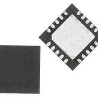
C8051F336-GMR Silicon Laboratories Inc, C8051F336-GMR Datasheet - Page 152

C8051F336-GMR
Manufacturer Part Number
C8051F336-GMR
Description
Microcontrollers (MCU) 16KB 10ADC 10DAC 768Ram MCU Lead Free
Manufacturer
Silicon Laboratories Inc
Datasheet
1.C8051F336-GM.pdf
(226 pages)
Specifications of C8051F336-GMR
Processor Series
C8051F3x
Core
8051
Data Bus Width
8 bit
Program Memory Type
Flash
Program Memory Size
16 KB
Data Ram Size
768 B
Interface Type
I2C, SPI, UART
Maximum Clock Frequency
25 MHz
Number Of Programmable I/os
17
Number Of Timers
4
Operating Supply Voltage
2.7 V to 3.6 V
Maximum Operating Temperature
+ 85 C
Mounting Style
SMD/SMT
Package / Case
QFN-20
3rd Party Development Tools
KSK-SL-TOOLSTICK, PK51, CA51, A51, ULINK2
Development Tools By Supplier
C8051F336DK
Minimum Operating Temperature
- 40 C
On-chip Adc
10 bit
On-chip Dac
10 bit
Package
20QFN
Device Core
8051
Family Name
C8051F336
Maximum Speed
25 MHz
Ram Size
768 Byte
Operating Temperature
-40 to 85 °C
Lead Free Status / Rohs Status
Details
Available stocks
Company
Part Number
Manufacturer
Quantity
Price
Company:
Part Number:
C8051F336-GMR
Manufacturer:
SILICON
Quantity:
100
Part Number:
C8051F336-GMR
Manufacturer:
SILICON LABS/芯科
Quantity:
20 000
Company:
Part Number:
C8051F336-GMR
Manufacturer:
SILICON
Quantity:
13 282
C8051F336/7/8/9
21.5.2. Read Sequence (Master)
During a read sequence, an SMBus master reads data from a slave device. The master in this transfer will
be a transmitter during the address byte, and a receiver during all data bytes. The SMBus interface gener-
ates the START condition and transmits the first byte containing the address of the target slave and the
data direction bit. In this case the data direction bit (R/W) will be logic 1 (READ). Serial data is then
received from the slave on SDA while the SMBus outputs the serial clock. The slave transmits one or more
bytes of serial data.
If hardware ACK generation is disabled, the ACKRQ is set to 1 and an interrupt is generated after each
received byte. Software must write the ACK bit at that time to ACK or NACK the received byte.
With hardware ACK generation enabled, the SMBus hardware will automatically generate the ACK/NACK,
and then post the interrupt. It is important to note that the appropriate ACK or NACK value should be
set up by the software prior to receiving the byte when hardware ACK generation is enabled.
Writing a 1 to the ACK bit generates an ACK; writing a 0 generates a NACK. Software should write a 0 to
the ACK bit for the last data transfer, to transmit a NACK. The interface exits Master Receiver Mode after
the STO bit is set and a STOP is generated. The interface will switch to Master Transmitter Mode if
SMB0DAT is written while an active Master Receiver. Figure 21.6 shows a typical master read sequence.
Two received data bytes are shown, though any number of bytes may be received. Notice that the ‘data
byte transferred’ interrupts occur at different places in the sequence, depending on whether hardware ACK
generation is enabled. The interrupt occurs before the ACK with hardware ACK generation disabled, and
after the ACK when hardware ACK generation is enabled.
152
S
Received by SMBus
Interface
Transmitted by
SMBus Interface
SLA
Figure 21.6. Typical Master Read Sequence
Interrupts with Hardware ACK Disabled (EHACK = 0)
Interrupts with Hardware ACK Enabled (EHACK = 1)
R
A
Data Byte
Rev.1.0
A
S = START
P = STOP
A = ACK
N = NACK
R = READ
SLA = Slave Address
Data Byte
N
P


