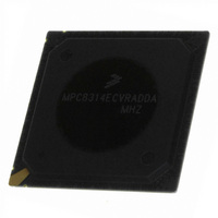
MPC8314ECVRADDA Freescale Semiconductor, MPC8314ECVRADDA Datasheet - Page 10

MPC8314ECVRADDA
Manufacturer Part Number
MPC8314ECVRADDA
Description
MPU POWERQUICC II PRO 620-PBGA
Manufacturer
Freescale Semiconductor
Datasheet
1.MPC8314VRADDA.pdf
(106 pages)
Specifications of MPC8314ECVRADDA
Processor Type
MPC83xx PowerQUICC II Pro 32-Bit
Speed
266MHz
Voltage
1V
Mounting Type
Surface Mount
Package / Case
620-PBGA
Processor Series
MPC8xxx
Core
e300
Data Bus Width
32 bit
Maximum Clock Frequency
50 MHz
Maximum Operating Temperature
+ 105 C
Mounting Style
SMD/SMT
Minimum Operating Temperature
- 40 C
Lead Free Status / RoHS Status
Lead free / RoHS Compliant
Features
-
Lead Free Status / Rohs Status
Lead free / RoHS Compliant
Available stocks
Company
Part Number
Manufacturer
Quantity
Price
Company:
Part Number:
MPC8314ECVRADDA
Manufacturer:
Freescale Semiconductor
Quantity:
135
Company:
Part Number:
MPC8314ECVRADDA
Manufacturer:
Freescale Semiconductor
Quantity:
10 000
Electrical Characteristics
Figure 2
3.1.3
Table 3
preliminary estimates.
3.2
The MPC8314E does not require the core supply voltage (VDD and VDDC) and I/O supply voltages
(GVDD, LVDDx_ON, LVDDx_OFF, NVDDx_ON and NVDDx_OFF) to be applied in any particular
order. During the power ramp up, before the power supplies are stable, if the I/O voltages are supplied
10
1
provides information on the characteristics of the output driver strengths. The values are
Local bus interface utilities signals
PCI signals
DDR signal
DDR2 signal 1
DUART, system control, I
GPIO signals
eTSEC
shows the undershoot and overshoot voltages at the interfaces of the MPC8314E.
Output Impedance can also be adjusted through configurable options in DDR Control Driver Register
(DDRCDR). See the MPC8315E PowerQUICC II Pro Host Processor Reference Manual .
Power Sequencing
Output Driver Characteristics
V
V
Note:
1
IH
1. t
IL
MPC8314E PowerQUICC
interface
Figure 2. Overshoot/Undershoot Voltage for GVDD/NVDD/LVDD
G/L/NVDD + 20%
G/L/NVDD + 5%
Driver Type
GND – 0.3 V
GND – 0.7 V
refers to the clock period associated with the bus clock interface.
G/L/NVDD
2
C, JTAG,SPI
GND
Table 3. Output Drive Capability
™
II Pro Processor Hardware Specifications, Rev. 0
Not to Exceed 10%
Output Impedance
of t
interface
(Ω)
42
25
18
18
42
42
42
1
LVDD = 3.3 V / 2.5 V
NVDD = 3.3 V
GVDD = 2.5 V
GVDD = 1.8 V
NVDD = 3.3 V
NVDD = 3.3 V
Voltage
Supply
Freescale Semiconductor


