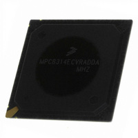
MPC8314ECVRADDA Freescale Semiconductor, MPC8314ECVRADDA Datasheet - Page 19

MPC8314ECVRADDA
Manufacturer Part Number
MPC8314ECVRADDA
Description
MPU POWERQUICC II PRO 620-PBGA
Manufacturer
Freescale Semiconductor
Datasheet
1.MPC8314VRADDA.pdf
(106 pages)
Specifications of MPC8314ECVRADDA
Processor Type
MPC83xx PowerQUICC II Pro 32-Bit
Speed
266MHz
Voltage
1V
Mounting Type
Surface Mount
Package / Case
620-PBGA
Processor Series
MPC8xxx
Core
e300
Data Bus Width
32 bit
Maximum Clock Frequency
50 MHz
Maximum Operating Temperature
+ 105 C
Mounting Style
SMD/SMT
Minimum Operating Temperature
- 40 C
Lead Free Status / RoHS Status
Lead free / RoHS Compliant
Features
-
Lead Free Status / Rohs Status
Lead free / RoHS Compliant
Available stocks
Company
Part Number
Manufacturer
Quantity
Price
Company:
Part Number:
MPC8314ECVRADDA
Manufacturer:
Freescale Semiconductor
Quantity:
135
Company:
Part Number:
MPC8314ECVRADDA
Manufacturer:
Freescale Semiconductor
Quantity:
10 000
Table 18
Figure 5
Freescale Semiconductor
At recommended operating conditions with GVDD of (1.8 V± 100 mV)
At recommended operating conditions with GVDD of (2.5V ± 200 mV)
Controller Skew for MDQS—MDQ
Note:
1. t
2. The amount of skew that can be tolerated from MDQS to a corresponding MDQ signal is called t
3. Memory controller ODT value of 150 Ω is recommended.
Controller Skew for MDQS—MDQ
Note:
1. t
2. The amount of skew that can be tolerated from MDQS to a corresponding MDQ signal is called t
MDQS[n]
captured with MDQS[n]. This should be subtracted from the total timing budget.
determined by the following equation: tDISKEW =+/–(T/4 – abs(t
absolute value of t
captured with MDQS[n]. This should be subtracted from the total timing budget.
determined by the following equation: t
absolute value of t
CISKEW
CISKEW
MDQ[x]
MCK[n]
MCK[n]
shows the DDR SDRAM input AC timing for the tolerated MDQS to MDQ skew (t
and
represents the total amount of skew consumed by the controller between MDQS[n] and any corresponding bit to be
represents the total amount of skew consumed by the controller between MDQS[n] and any corresponding bit to be
Table 19
CISKEW
CISKEW
MPC8314E PowerQUICC
Parameter
Parameter
lists the input AC timing specifications for the DDR SDRAM interface.
.
.
Table 18. DDR2 SDRAM Input AC Timing Specifications
Table 19. DDR SDRAM Input AC Timing Specifications
Figure 5. Timing Diagram for t
DISKEW
t
t
MCK
DISKEW
266 MHz
200 MHz
266 MHz
200 MHz
™
=+/–(T/4 – abs(t
II Pro Processor Hardware Specifications, Rev. 0
D0
Symbol
Symbol
t
t
CISKEW
CISKEW
CISKEW
CISKEW
D1
)) where T is the clock period and abs(t
)) where T is the clock period and abs(t
t
DISKEW
DISKEW
–1250
–1250
–875
–750
Min
Min
1250
1250
Max
Max
875
750
DISKEW
DISKEW
DDR and DDR2 SDRAM
.This can be
. This can be
Unit
Unit
ps
ps
CISKEW
CISKEW
DISKEW
Notes
1, 2, 3
Notes
) is the
) is the
1, 2
)
19


