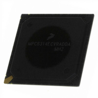
MPC8314ECVRADDA Freescale Semiconductor, MPC8314ECVRADDA Datasheet - Page 11

MPC8314ECVRADDA
Manufacturer Part Number
MPC8314ECVRADDA
Description
MPU POWERQUICC II PRO 620-PBGA
Manufacturer
Freescale Semiconductor
Datasheet
1.MPC8314VRADDA.pdf
(106 pages)
Specifications of MPC8314ECVRADDA
Processor Type
MPC83xx PowerQUICC II Pro 32-Bit
Speed
266MHz
Voltage
1V
Mounting Type
Surface Mount
Package / Case
620-PBGA
Processor Series
MPC8xxx
Core
e300
Data Bus Width
32 bit
Maximum Clock Frequency
50 MHz
Maximum Operating Temperature
+ 105 C
Mounting Style
SMD/SMT
Minimum Operating Temperature
- 40 C
Lead Free Status / RoHS Status
Lead free / RoHS Compliant
Features
-
Lead Free Status / Rohs Status
Lead free / RoHS Compliant
Available stocks
Company
Part Number
Manufacturer
Quantity
Price
Company:
Part Number:
MPC8314ECVRADDA
Manufacturer:
Freescale Semiconductor
Quantity:
135
Company:
Part Number:
MPC8314ECVRADDA
Manufacturer:
Freescale Semiconductor
Quantity:
10 000
before the core voltage, there may be a period of time when all input and output pins be actively driven
and cause contention and/or excessive current. In order to avoid actively driving the I/O pins and to
eliminate excessive current draw, apply the continuous core voltage (VDDC) before the continuous I/O
voltages (LVDDx_ON and NVDDx_ON) and switchable core voltage (VDD) before the switchable I/O
voltages (GVDD, LVDDx_OFF, and NVDDx_OFF). PORESET should be asserted before the continuous
power supplies fully ramp up. In the case where the core voltage is applied first, the core voltage supply
must rise to 90% of its nominal value before the I/O supplies reach 0.7 V, see
supplies are stable, wait for a minimum of 32 clock cycles before negating PORESET.
The I/O power supply ramp-up slew rate should be slower than 4V/100
circuit
Figure 3
When switching from normal mode to D3 warm (standby) mode, first turn off the switchable I/O voltage
supply and then turn off the switchable core voltage supply. Similarly, when switching from D3 warm
(standby) mode to normal mode, first turn on the switchable core voltage supply and then turn on the
switchable I/O voltage supply.
Freescale Semiconductor
90%
V
.
Power sequence for continuous power supplies
shows the power-up sequencing for switchable and continuous supplies.
When the device is in D3 warm (standby) mode, all external voltage
supplies applied to any I/O pins, with the exception of wake-up pins, must
be turned off. Applying supplied external voltage to any I/O pins, except the
wake up pins, while the device is in D3 warm standby mode may cause
permanent damage to the device.
MPC8314E PowerQUICC
Continuous I/O Voltage
Continuous Core Voltage
Figure 3. Power-Up Sequencing
0.7 V
t
™
II Pro Processor Hardware Specifications, Rev. 0
CAUTION
90%
V
Power sequence for switchable power supplies
μ
s, this requirement is for ESD
Figure
Switchable I/O Voltage
Switchable Core Voltage (VDD)
3. Once all the power
Electrical Characteristics
0.7 V
t
11


