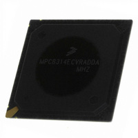
MPC8314ECVRADDA Freescale Semiconductor, MPC8314ECVRADDA Datasheet - Page 8

MPC8314ECVRADDA
Manufacturer Part Number
MPC8314ECVRADDA
Description
MPU POWERQUICC II PRO 620-PBGA
Manufacturer
Freescale Semiconductor
Datasheet
1.MPC8314VRADDA.pdf
(106 pages)
Specifications of MPC8314ECVRADDA
Processor Type
MPC83xx PowerQUICC II Pro 32-Bit
Speed
266MHz
Voltage
1V
Mounting Type
Surface Mount
Package / Case
620-PBGA
Processor Series
MPC8xxx
Core
e300
Data Bus Width
32 bit
Maximum Clock Frequency
50 MHz
Maximum Operating Temperature
+ 105 C
Mounting Style
SMD/SMT
Minimum Operating Temperature
- 40 C
Lead Free Status / RoHS Status
Lead free / RoHS Compliant
Features
-
Lead Free Status / Rohs Status
Lead free / RoHS Compliant
Available stocks
Company
Part Number
Manufacturer
Quantity
Price
Company:
Part Number:
MPC8314ECVRADDA
Manufacturer:
Freescale Semiconductor
Quantity:
135
Company:
Part Number:
MPC8314ECVRADDA
Manufacturer:
Freescale Semiconductor
Quantity:
10 000
Electrical Characteristics
3.1.2
Table 2
are the recommended and tested operating conditions. Proper device operation outside of these conditions
is not guaranteed.
8
PHY voltage
Input voltage
Storage temperature range
Notes:
1. Functional and tested operating conditions are given in
2. Caution: MV
3. Caution: (N,L)V
4. (M,N,L)V
5. NV
6. The max value of supply voltage shoud be selected based on the RGMII mode.
7. NVDD means NVDD1_OFF, NVDD1_ON, NVDD2_OFF, NVDD2_ON, NVDD3_OFF, NVDD4_OFF
8. LVDD means LVDD1_OFF and LVDD2_ON
SerDes internal digital power
SerDes internal digital power
SerDes I/O digital power
functional operation at the maximums is not guaranteed. Stresses beyond those listed may affect device reliability or cause
permanent damage to the device.
power-on reset and power-down sequences.
during power-on reset and power-down sequences.
shown in Figure 3.
IN
provides the recommended operating conditions for theMPC8314E. Note that the values in
on the PCI interface may overshoot/undershoot according to the PCI Electrical Specification for 3.3-V operation, as
IN
Power Supply Voltage Specification
and MVREF may overshoot/undershoot to a voltage and for a maximum duration as shown in
IN
Characteristic
must not exceed GVDD by more than 0.3 V. This limit may be exceeded for a maximum of 20 ms during
IN
USB PHY
SERDES PHY
DDR DRAM signals
DDR DRAM reference
eTSEC signals
Local bus, DUART, SYS_CLKIN, system
control and power management, I
JTAG signals
PCI
must not exceed (N,L)VDD by more than 0.3 V. This limit may be exceeded for a maximum of 20 ms
MPC8314E PowerQUICC
Characteristic
Table 1. Absolute Maximum Ratings
Table 2. Recommended Operating Conditions
™
II Pro Processor Hardware Specifications, Rev. 0
XCOREVDD
XCOREVSS
2
XPADVDD
C, and
Symbol
Table
USB_VDDA_BIAS,
USB_PLL_PWR3,
2. Absolute maximum ratings are stress ratings only, and
USB_PLL_PWR1
XCOREVDD,
XPADVDD,
SDAVDD
Symbol
MVREF
VDDA
MV
T
NV
NV
LV
Recommended
STG
IN
1.0 ± 50 mv
1.0 ± 50 mv
IN
IN
IN
Value
1
0.0
(continued)
1
–0.3 to (GVDD + 0.3)
–0.3 to (GVDD + 0.3)
–0.3 to (NVDD + 0.3)
–0.3 to (NVDD + 0.3)
–0.3 to (LVDD + 0.3)
–0.3 to 1.26
–0.3 to 1.26
Max Value
–0.3 to 3.6
Unit
–55 to150
V
V
V
Status in D3
Warm mode
Switched Off
Switched Off
Freescale Semiconductor
—
Figure
Unit
°C
V
V
V
V
V
V
V
V
2.
Notes
Table 2
—
—
—
Notes
2, 4
2, 4
3, 4
3, 4
—
—
—
—
5


