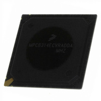
MPC8314ECVRADDA Freescale Semiconductor, MPC8314ECVRADDA Datasheet - Page 38

MPC8314ECVRADDA
Manufacturer Part Number
MPC8314ECVRADDA
Description
MPU POWERQUICC II PRO 620-PBGA
Manufacturer
Freescale Semiconductor
Datasheet
1.MPC8314VRADDA.pdf
(106 pages)
Specifications of MPC8314ECVRADDA
Processor Type
MPC83xx PowerQUICC II Pro 32-Bit
Speed
266MHz
Voltage
1V
Mounting Type
Surface Mount
Package / Case
620-PBGA
Processor Series
MPC8xxx
Core
e300
Data Bus Width
32 bit
Maximum Clock Frequency
50 MHz
Maximum Operating Temperature
+ 105 C
Mounting Style
SMD/SMT
Minimum Operating Temperature
- 40 C
Lead Free Status / RoHS Status
Lead free / RoHS Compliant
Features
-
Lead Free Status / Rohs Status
Lead free / RoHS Compliant
Available stocks
Company
Part Number
Manufacturer
Quantity
Price
Company:
Part Number:
MPC8314ECVRADDA
Manufacturer:
Freescale Semiconductor
Quantity:
135
Company:
Part Number:
MPC8314ECVRADDA
Manufacturer:
Freescale Semiconductor
Quantity:
10 000
USB
10.1.1
Table 39
10.1.2
Table 40
Figure 21
38
High-level input voltage
Low-level input voltage
Input current
High-level output voltage, I
Low-level output voltage, I
Note:
1. The symbol V
USB clock cycle time
Input setup to USB clock—all inputs
Input hold to USB clock—all inputs
USB clock to output valid—all outputs
Output hold from USB clock—all outputs
Notes:
1. The symbols used for timing specifications follow the pattern of t
2. All timings are in reference to USB clock.
3. All signals are measured from NVDD/2 of the rising edge of USB clock to 0.4 × NVDD of the signal in question for 3.3-V
4. Input timings are measured at the pin.
5. For purposes of active/float timing measurements, the Hi-Z or off-state is defined to be when the total current delivered
inputs and t
(US) for the input (I) to go invalid (X) with respect to the time the USB clock reference (K) goes high (H). Also, t
symbolizes USB timing (US) for the us clock reference (K) to go high (H), with respect to the output (O) going invalid (X) or
output hold time.
signaling levels.
through the component pin is less than or equal to the leakage current specification.
lists the DC electrical characteristics for the USB interface.
lists the general timing parameters of the USB-ULPI interface.
and
USB DC Electrical Characteristics
USB AC Electrical Specifications
(First two letters of functional block)(reference)(state)(signal)(state)
IN
Figure 22
, in this case, represents the NV
MPC8314E PowerQUICC
Parameter
OL
OH
Output
Parameter
= 100 μA
provide the AC test load and signals for the USB, respectively.
= –100 μA
Table 39. USB DC Electrical Characteristics
Table 40. USB General Timing Parameters
Figure 21. USB AC Test Load
Z
™
0
IN
II Pro Processor Hardware Specifications, Rev. 0
= 50 Ω
symbol referenced in
Symbol
t
t
t
t
USKHOV
USKHOX
USIVKH
USIXKH
t
USCK
(First two letters of functional block)(signal)(state)(reference)(state)
for outputs. For example, t
Symbol
1
V
V
V
V
I
Table 1
OH
IN
OL
IH
IL
R
L
= 50 Ω
Min
15
—
4
1
1
and
LVDD – 0.2
Table
–0.3
Min
—
—
2
NVDD/2
2.
USIXKH
Max
—
—
—
—
9
Freescale Semiconductor
LVDD + 0.3
symbolizes USB timing
Max
0.8
0.2
±5
—
Unit
ns
ns
ns
ns
ns
USKHOX
Notes
Unit
1, 2
1, 4
1, 4
μA
V
V
V
V
1
1
for


